Optoelectronic Junction Devices | Physics Class 12 - NEET PDF Download

Opto electronic junction devices
The semiconductor diodes in which the current carriers are generated by the photons(through photo excitation) is called optoelectronic devices Some of the opto electronic junction devices are –Photodiode, Light emitting diode and solar cell.
Photodiode – Electron-hole pair is generated due to the illumination of the junction with light.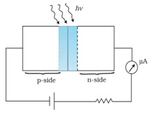
Light emitting diode – When forward biased properly, this special p-n junction emits light radiation continuously.
Solar cell–When solar light falls on p-n junction, it generates emf which can be used effectively.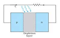
Photodiode
Application – Photodiodes are used for detecting optical signal or they act as photo detectors
➤ Circuit Diagram
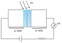
- This is a special p-n junction diode made up of photosensitive semiconducting material
- The diode has a transparent window to allow light to fall on the diode
➤ Working
- It is operated under reverse bias below the breakdown voltage.
- When photodiode is illuminated with light (photons), with energy hט greater than the energy gap of the semiconductor, the electron-hole pairs are generated due to the absorption of photons, in or near the depletion region of the diode.
- Due to electric field at the junction, electrons and holes are separated before they combine.
- The direction of electric field is such that the electrons reach n-side and the holes reach the p-side.
- The movement of electrons and holes gives rise to emf.
- When external load is connected, current flows. The magnitude of the photocurrent depends on the intensity of incident light.
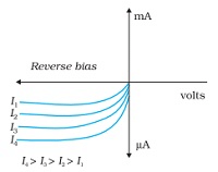
- In reverse bias, we can observe that as intensity increases, the current also increases.
➤ Characteristics
- The characteristic of a photodiode is shown below:
Problem: A p-n photodiode is fabricated from a semiconductor with band gap of 2.8 eV. Can it detect a wavelength of 6000 nm?
Solution : Eg = 2.8 eV; λ = 600 nm = 600 * 10-9
We know, Energy E = hc / λ
= 6.6 * 10-34 * 3 * 108 / 600 * 10-9 * 1.6 * 10-19 eV
= 2.06 eV
As E < Eg, 2.06 < 2.8 eV so p-n junction cannot detect the radiation of given wavelength
Light emitting diode
Application – They convert electrical energy into light
- It is a heavily doped p-n junction which under forward bias emits spontaneous radiation.
- The diode is encapsulated with a transparent cover so that the emitted light can come out.
- When the diode is forward biased, the electrons are sent from n layer to p layer and the holes are sent from p to n.
- Thus, at the boundary due to forward bias, the concentration of the minority carriers increases.
- The excess minority carriers recombine with the majority carriers, near the junction.
- On recombination, energy is released in the form of photons.
- Photons with energy equal to or slightly less than the band gap is emitted.
- When the forward current of the diode is small, the intensity of the light emitted is small.
- As the forward current increases, the intensity of light increases and reaches maximum.
- Further increase in forward current, results in the decrease of light intensity.
- LEDs are thus biased in such a way such that the efficiency is maximum.
- The reverse breakdown voltage of LED is very small (say) 5V. Proper precaution should be taken such that high reverse voltage do not appear across them.
- LEDs have the following advantages over the conventional lamps:
(i) Low operational voltage and less power
(ii) Fast action and no warm-up time required
(iii) Long life
(iv) Fast on-off switching capacity
Solar cell
Principle–These photo voltaic devices convert the optical radiation into electricity.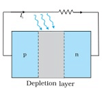
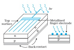
Circuit
- When solar light falls on a p-n junction, it generates emf.
- As the solar radiation is incident at the junction, the junction area is kept much larger for more power generation.
- A p Si layer of about 300 * 10-6m is taken. About this a still thin layer of about 0.3 * 10-6 m n Si layer is grown on one side by the process of diffusion.
- The other side of the p-layer is coated with a metal. This servers as a back contact.
- On the top of n Si layer, metallic grid is deposited. This is called front contact.
- The light is incident on the grid from the top.
Working
- The generation of emf by the solar cell, when light falls on, is due to the following three basic processes – (a) generation (b) separation and (c) collection
- Generation
– The generation of electron-hole paid due to light with energy hט> Eg close to the junction. - Separation
– The separation of electrons and holes due to the electric field of the depletion region.
– The electrons are swept to the n-side and the holes to the p-side. - Collection
– The electrons reaching the n-side are collected by the front contact and holes reaching the p-side are collected by the back contact.
– Thus, the p-side becomes positive and the n-side becomes negative giving rise to photo voltage.
– When external load is connected, a photo current IL flows through the load.
Graph
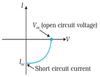
- The graph showing the VI characteristics, with V along the X-axis and I along the Y-axis is as given above.
- The graph is indicated in the fourth quadrant as solar cell does not draw current but supplies the same to the load.
Application
- Solar cells are used in power electronic devices in satellites and space vehicles.
- They are also used as power supply in calculators.
Criteria for material selection of material for solar cell
- Band gap between 1.0 and 1.8 eV.
- High optical absorption.
- Electrical conductivity.
- Availability of raw material.
- Cost effective.
|
74 videos|314 docs|88 tests
|
FAQs on Optoelectronic Junction Devices - Physics Class 12 - NEET
| 1. What are opto electronic junction devices? |  |
| 2. How do opto electronic junction devices work? | |
| 3. What are some common applications of opto electronic junction devices? | |
| 4. What are the advantages of using opto electronic junction devices? | |
| 5. How are opto electronic junction devices different from traditional electronic devices? | |


MCQs
,video lectures
,Viva Questions
,Optoelectronic Junction Devices | Physics Class 12 - NEET
,Free
,Exam
,Objective type Questions
,Optoelectronic Junction Devices | Physics Class 12 - NEET
,Previous Year Questions with Solutions
,Sample Paper
,past year papers
,mock tests for examination
,Summary
,Extra Questions
,ppt
,practice quizzes
,Important questions
,study material
,Optoelectronic Junction Devices | Physics Class 12 - NEET
,Semester Notes
,shortcuts and tricks
;


Optoelectronic Junction Devices Free PDF Download
Importance of Optoelectronic Junction Devices
Optoelectronic Junction Devices Notes
Optoelectronic Junction Devices NEET Questions
Study Optoelectronic Junction Devices on the App
|
© EduRev
|
Education Revolution
|


|


