Carrier Transport | Electronic Devices - Electronics and Communication Engineering (ECE) PDF Download

Introduction
In semiconductors, current arises from the motion of free carriers, driven by two mechanisms: carrier drift and carrier diffusion.
- Carrier drift: Caused by an electric field from an applied voltage, charged carriers accelerate, then reach a constant average velocity (v) due to collisions with impurities and lattice vibrations. The velocity-to-field ratio is mobility. At high fields, velocity saturates at the saturation velocity. Surface or interface scattering reduces mobility.
- Carrier diffusion: Driven by thermal energy, carriers move from high to low density regions, creating a gradient via doping variations or thermal gradients.
- Total current: Sum of drift and diffusion currents.
Both mechanisms involve the same particles and scattering, linking mobility and diffusion constant through the Einstein relation.
Recombination
A process whereby electrons and holes are annihilated or destroyed.Energy Bands in Recombination Processes
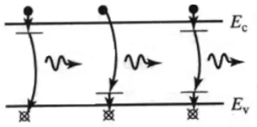
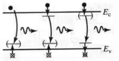
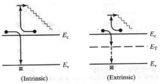
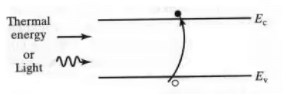
- Band-to-Band Recombination: Also referred to as direct thermal recombination, is the direct annihilation of a conduction band electron and a valence band hole. The electron falls from an allowed conduction band state into a vacant valence band state. This process is typically radiative with the excess energy released during the process going into the production of a photon (light).
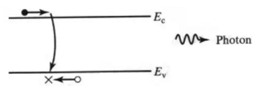 Band-to-Band Recombination
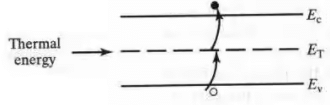
 - R-G Center Recombination: A defect often causes an energy state in the mid-gap region of the bandgap that can act as traps for carriers. In this process, a conduction band electron gets trapped at this defect and energy state and then a valence band hole is trapped and recombines with the electron or vice versa. This process is typically nonradiative.
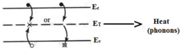 R-G Center Recombination
 - Recombination via Shallow Levels: Donor and acceptor sites can also act as intermediaries in the recombination process similar to the R-G Center recombination with the exception that the recombination is quite often radiative.
 Recombination via Shallow Levels
 - Recombination Involving Excitons: Conduction band electrons and valence band holes can form a slightly lower energy state by becoming bound to each other in a hydrogen-like arrangement. The electron and hole can then recombine and result in a photon that has energy slightly less than the bandgap.
 Recombination Involving Excitons
 - Auger Recombination: A nonradioactive recombination event where a conduction band electron loses energy to another conduction band electron which gains energy to result in one electron recombining with a hole in the valence band and one high energy electron which rapidly loses energy by phonon emission and relaxes back down to the conduction band.
 Auger Recombination
Generation
A process whereby electrons and holes are created.
- The recombination processes can be reversed resulting in generation processes.
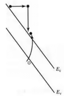
- Band-to-Band generation occurs when an electron from the valence band is excited by light or heat to the conduction band.
 Band-to-Band generation
 - Generation of an electron and hole by an R-G centre intermediary can be done in a couple of ways including an electron from the valence band being excited to the trap state and then to the conduction band creating a hole in the valence band and electron in the conduction band.
 R-G Centre generation
 - Also, an electron in the trap state can be excited to the conduction band while the hole is excited to the valence band.
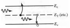 Photoemission from band gap centers
 - Another common carrier generation is carrier generation via impact ionization where a high energy electron loses energy to produce an electron-hole pair.
 Carrier Generation via impact ionization
Carrier Diffusion
- Diffusion: particle movement in response to concentration gradient
- Elements of diffusion:
- a medium (Si crystal)
- a gradient of particles (electrons and holes) inside the medium
- collisions between particles and medium send particles off in random directions: → overall, particle movement down the gradient.
Key diffusion relationship (Fick’s first law):
- Diffusion flux ∝ - concentration gradient
- Flux ≡ number of particles crossing unit area per unit time [cm−2 · s−1]
- For electrons:

- For holes:
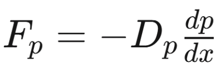
- Dn ≡ electron diffusion coefficient [cm2/s]
- Dp ≡ hole diffusion coefficient [cm2/s]
- D measures the ease of carrier diffusion in response to a concentration gradient: D ↑ ⇒ Fdi ff ↑
- Diffusion current density = charge × carrier flux
Carrier Drift
- Net velocity of the charged particles ⇒ electric current.
- Drift current density ∝ carrier drift velocity ∝ carrier concentration ∝ carrier charge.
- Drift currents:
Jndri ft = -qnvdn = qnμnE
Jpdri ft = -qnvdp = qnμpE
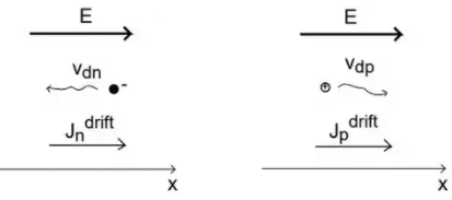
- Total drift current:
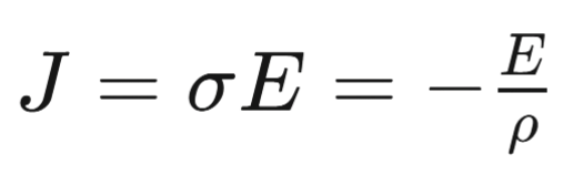
Jdri ft = Jndri ft + Jpdri ft = q(nμn + pμp)E - Has the shape of Ohm’s Law:
- Where:
σ ≡ conductivity[Ω-1. cm-1]
ρ ≡ resistivity [Ω . cm] - Then:
- Einstein's Relation: In a semiconductor, this relation gives the relationship between diffusion constant, mobility and thermal voltage.
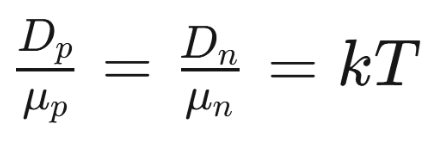 VT = KT and is 26mV at 27°C
 - Mobility:
- The electron mobility and hole mobility have a similar doping dependence: For low doping concentrations, the mobility is almost constant and is primarily limited by phonon scattering. At higher doping concentrations, the mobility decreases due to ionized impurity scattering with the ionized doping atoms. The actual mobility also depends on the type of dopant.
- Mobility is linked to the total number of ionized impurities or the sum of the donor and acceptor densities.
- The minority carrier mobility also depends on the total impurity density. The minority-carrier mobility can be approximated by the majority-carrier mobility in a material with the same number of impurities.
- The mobility at a particular doping density is obtained from the following empiric expression: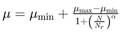
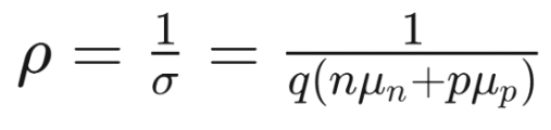
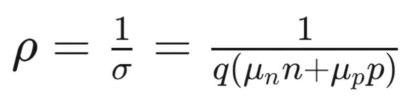
- Resistivity:
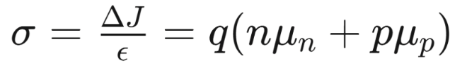
- The resistivity is defined as the inverse of the conductivity. The conductivity of a material is defined as the current density divided by the applied electric field. Since the current density equals the product of the charge of the mobile carriers.
- To include the contribution of electrons as well as holes to the conductivity, we add the current density due to holes to that of the electrons.
- or:
J = qnve + qpvh = q(nμn + pμp)∈ - The conductivity due to electrons and holes is then obtained from:
- The resistivity is:
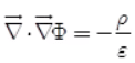
Poisson’s Equation
- Poisson's equation correlates the electrostatic potential Φ to a given charge distribution ρ.
- Using the relation between the electric displacement vector and the electric field vector,
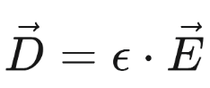
- where ε is the permittivity tensor. This relation is valid for materials with time independent permittivity. As materials used in semiconductor devices normally do not show significant anisotropy of the permittivity, can be considered as a scalar quantity ε in device simulation. The total permittivity is obtained from the relative εr and the vacuum permittivity ε0 as ε = εr ε0.
As
- can be expressed as a gradient field of a scalar potential field.
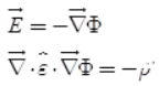
- Consider the permittivity a scalar, which is constant in homogeneous materials, we obtain Poisson's equation.
- The space charge density ρ consists of :
ρ = q(p – n + C), - where q is the elementary charge, p and n the hole and electron concentrations, respectively, and the concentration of additional, typically fixed, charges. These fixed charges can originate from charged impurities of donor (ND) and acceptor (NA) type and from trapped holes (ρp) and electrons (ρn),
C = ND – NA + ρp - ρn - Poisson's equation commonly used for semiconductor device simulation:
 -q/∈(p - n + Nd - NA - ρp = ρn)
Continuity Equations
- The continuity equations can be derived using the following:
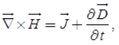
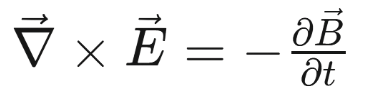
- By applying the divergence operator:
 , to the equation and considering that the divergence of the curl of any vector field equals zero.
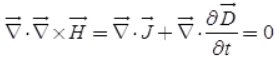
- Separating the total current density
 into hole and electron current densities,
 - and
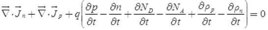
- When we consider the charged impurities as time-invariant and introduce a quantity to split up the above equation into separate equations for electrons and holes, we get
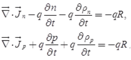
- The quantity R gives the net recombination rate for electrons and holes.
- A positive value means recombination.
- A negative value means the generation of carriers.
The document Carrier Transport | Electronic Devices - Electronics and Communication Engineering (ECE) is a part of the Electronics and Communication Engineering (ECE) Course Electronic Devices.
All you need of Electronics and Communication Engineering (ECE) at this link: Electronics and Communication Engineering (ECE)
|
43 docs|29 tests
|
FAQs on Carrier Transport - Electronic Devices - Electronics and Communication Engineering (ECE)
| 1. What is carrier transport in electronics and communication engineering? |  |
Ans. Carrier transport refers to the movement of charge carriers, such as electrons or holes, through a conductive material or a semiconductor. In electronics and communication engineering, understanding carrier transport is crucial for designing and analyzing electronic devices and systems.
| 2. How does carrier transport affect the performance of electronic devices? | |
Ans. The efficiency and performance of electronic devices depend on the speed and accuracy of carrier transport. If carriers encounter obstacles or experience high resistance during transport, it can lead to signal degradation, reduced device efficiency, and even device failure.
| 3. What are the main factors that influence carrier transport in electronic devices? | |
Ans. There are several factors that influence carrier transport in electronic devices. Some of the main factors include the material properties of the conductive medium or semiconductor, temperature, electric field strength, impurities or defects in the material, and the presence of external forces or magnetic fields.
| 4. How can carrier transport be improved in electronic devices? | |
Ans. To improve carrier transport in electronic devices, engineers employ various techniques. These include optimizing the material properties, reducing impurities and defects, designing efficient pathways for carrier flow, implementing advanced fabrication processes, and utilizing external means such as doping or applying electric or magnetic fields to enhance carrier mobility.
| 5. What are some common techniques used to analyze and study carrier transport in electronic devices? | |
Ans. Engineers and researchers use various techniques to analyze and study carrier transport in electronic devices. Some common techniques include Hall effect measurements, impedance spectroscopy, current-voltage (IV) characterization, capacitance-voltage (CV) measurements, and numerical simulations using device modeling software. These techniques provide valuable insights into carrier behavior, device performance, and potential areas of improvement.
About this Document

1.6K Views

4.89/5
Rating

Oct 14, 2025
Last updated
Related Exams
Document Description: Carrier Transport for Electronics and Communication Engineering (ECE) 2025 is part of Electronic Devices preparation.
The notes and questions for Carrier Transport have been prepared according to the Electronics and Communication Engineering (ECE) exam syllabus. Information about Carrier Transport covers topics
like Introduction, Recombination and Carrier Transport Example, for Electronics and Communication Engineering (ECE) 2025 Exam. Find important definitions, questions, notes, meanings, examples, exercises and tests below for Carrier Transport.
Introduction of Carrier Transport in English is available as part of our Electronic Devices
for Electronics and Communication Engineering (ECE) & Carrier Transport in Hindi for Electronic Devices course.
Download more important topics related with notes, lectures and mock test series for Electronics and Communication Engineering (ECE)
Exam by signing up for free. Electronics and Communication Engineering (ECE): Carrier Transport | Electronic Devices - Electronics and Communication Engineering (ECE)
Description
Full syllabus notes, lecture & questions for Carrier Transport | Electronic Devices - Electronics and Communication Engineering (ECE) - Electronics and Communication Engineering (ECE) | Plus excerises question with solution to help you revise complete syllabus for Electronic Devices | Best notes, free PDF download
Information about Carrier Transport
In this doc you can find the meaning of Carrier Transport defined & explained in the simplest way possible. Besides explaining types of
Carrier Transport theory, EduRev gives you an ample number of questions to practice Carrier Transport tests, examples and also practice Electronics and Communication Engineering (ECE)
tests

Related Searches
Carrier Transport | Electronic Devices - Electronics and Communication Engineering (ECE)
,mock tests for examination
,Semester Notes
,study material
,video lectures
,Objective type Questions
,Viva Questions
,past year papers
,practice quizzes
,Carrier Transport | Electronic Devices - Electronics and Communication Engineering (ECE)
,Extra Questions
,shortcuts and tricks
,ppt
,Summary
,Free
,Sample Paper
,Important questions
,MCQs
,Carrier Transport | Electronic Devices - Electronics and Communication Engineering (ECE)
,Previous Year Questions with Solutions
,Exam
;


Additional Information about Carrier Transport for Electronics and Communication Engineering (ECE) Preparation
Carrier Transport Free PDF Download
The Carrier Transport is an invaluable resource that delves deep into the core of the Electronics and Communication Engineering (ECE) exam.
These study notes are curated by experts and cover all the essential topics and concepts, making your preparation more efficient and effective.
With the help of these notes, you can grasp complex subjects quickly, revise important points easily,
and reinforce your understanding of key concepts. The study notes are presented in a concise and easy-to-understand manner,
allowing you to optimize your learning process. Whether you're looking for best-recommended books, sample papers, study material,
or toppers' notes, this PDF has got you covered. Download the Carrier Transport now and kickstart your journey towards success in the Electronics and Communication Engineering (ECE) exam.
Importance of Carrier Transport
The importance of Carrier Transport cannot be overstated, especially for Electronics and Communication Engineering (ECE) aspirants.
This document holds the key to success in the Electronics and Communication Engineering (ECE) exam.
It offers a detailed understanding of the concept, providing invaluable insights into the topic.
By knowing the concepts well in advance, students can plan their preparation effectively.
Utilize this indispensable guide for a well-rounded preparation and achieve your desired results.
Carrier Transport Notes
Carrier Transport Notes offer in-depth insights into the specific topic to help you master it with ease.
This comprehensive document covers all aspects related to Carrier Transport.
It includes detailed information about the exam syllabus, recommended books, and study materials for a well-rounded preparation.
Practice papers and question papers enable you to assess your progress effectively.
Additionally, the paper analysis provides valuable tips for tackling the exam strategically.
Access to Toppers' notes gives you an edge in understanding complex concepts.
Whether you're a beginner or aiming for advanced proficiency, Carrier Transport Notes on EduRev are your ultimate resource for success.
Carrier Transport Electronics and Communication Engineering (ECE) Questions
The "Carrier Transport Electronics and Communication Engineering (ECE) Questions" guide is a valuable resource for all aspiring students preparing for the
Electronics and Communication Engineering (ECE) exam. It focuses on providing a wide range of practice questions to help students gauge
their understanding of the exam topics. These questions cover the entire syllabus, ensuring comprehensive preparation.
The guide includes previous years' question papers for students to familiarize themselves with the exam's format and difficulty level.
Additionally, it offers subject-specific question banks, allowing students to focus on weak areas and improve their performance.
Study Carrier Transport on the App
Students of Electronics and Communication Engineering (ECE) can study Carrier Transport alongwith tests & analysis from the EduRev app,
which will help them while preparing for their exam. Apart from the Carrier Transport,
students can also utilize the EduRev App for other study materials such as previous year question papers, syllabus, important questions, etc.
The EduRev App will make your learning easier as you can access it from anywhere you want.
The content of Carrier Transport is prepared as per the latest Electronics and Communication Engineering (ECE) syllabus.
|
© EduRev
|
Education Revolution
|


|


Signup on EduRev and stay on top of your study goals
10M+ students crushing their study goals daily