Frequency Response

Frequency Response of Amplifiers
- An amplifier's gain is not the same at all frequencies; the variation of gain with frequency is called the amplifier's frequency response.
- Every amplifier provides adequate amplification only over a band of frequencies called the passband or mid-band. Frequencies below and above this band are attenuated.
- Examples: an amplifier designed for radio frequencies will amplify signals above about 100 kHz but will not amplify low-frequency audio; an audio amplifier will pass frequencies in the audio band but will attenuate high RF signals.
- Key terms:
- Lower cut-off frequency (f1) - the frequency where the gain falls by 3 dB from its mid-band value on the low-frequency side.
- Upper cut-off frequency (f2) - the frequency where the gain falls by 3 dB from its mid-band value on the high-frequency side.
- Bandwidth (BW) - the difference f2 - f1; for many amplifiers mid-band response is used where gain is approximately constant.
- Mid-band gain - the gain in the frequency region between f1 and f2 where reactive effects are negligible.
- 3-dB point - a standard reference point where the power is half (voltage gain falls by 1/√2 ≈ 0.707 of mid-band value).
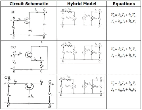
Hybrid Equivalent Circuit for a Transistor
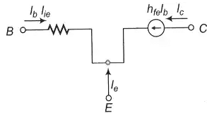
For small-signal analysis a single-stage transistor amplifier (common-base, common-emitter or common-collector) can be represented by a standard hybrid model. The hybrid equivalent places a Thevenin equivalent at the input and a Norton equivalent at the output, and uses h-parameters to relate small changes of voltages and currents.
- The basic small-signal h-parameter relations (voltage and current equations) for the two-port transistor model are shown in the schematic and equations below.

- Definitions of the h-parameters:
- hi - input impedance (also written hie, hib etc. depending on connection).
- hr - reverse voltage ratio (voltage feedback from output to input).
- hf - forward current transfer ratio (near the small-signal current gain).
- h0 - output admittance (inverse of output resistance).
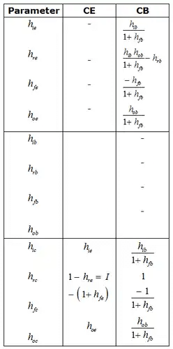
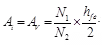
- The h-parameters carry a second subscript (b, e or c) to indicate the amplifier configuration (CB, CE or CC) for which they were measured.
- h-parameters may be obtained from transistor characteristic curves or measured experimentally under small-signal AC conditions. Typical measured tables are useful for design.
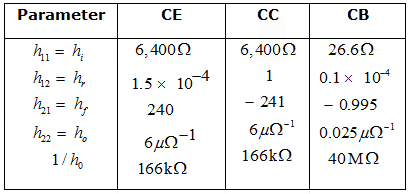
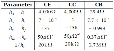
- If h-parameters are known for one connection but required for another, approximate conversion formulae may be used to convert between CB, CE and CC forms.
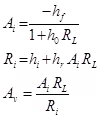
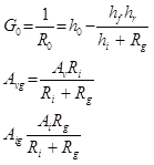
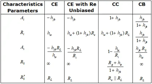
- Knowing the h-parameters and the external resistances Rg and RL, one can compute small-signal performance quantities such as:
- Ai - current gain
- Ri - input resistance
- Av - voltage gain
- Ro - output resistance
- Avg and Aig - gains including source or load effects.
- For power applications one can use h-parameters to find conditions for Maximum Available Power Gain (MAG) and to perform dually matched source and load calculations.
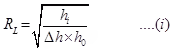
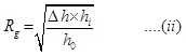
- Where Δh = hi ho - hr hf.
- The hybrid circuit schematic and the V-I and h-parameter equations for CE, CC and CB connections are summarised below.
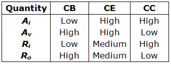
- A transistor amplifier's characteristics depend strongly upon Rg and RL. A comparison of typical behaviour for CB, CE and CC connections is useful when selecting a configuration.
- Approximate expressions for Ai, Ri, Av and Ro in terms of CE h-parameters are valid when hoe RL ≤ 0.1 (i.e. output admittance times load is small).
- Under the further approximation that the output admittance is negligible, one may set hoe ≈ 0 and simplify the expressions.
Low-Frequency Response of Amplifiers
The low-frequency response is dominated by coupling capacitors, bypass capacitors and transformer primary inductances. These reactive elements create high-pass behaviour that increases the amplifier's gain as frequency rises from DC until the mid-band is reached.
- In a single-stage common-emitter amplifier, the emitter bypass capacitor must be sufficiently large to keep the lower 3-dB frequency f1 small. Approximate expressions for f1 under different circuit conditions are summarised here:
- Electrolytic losses in the emitter bypass capacitor can degrade the low-frequency response and also reduce the mid-band gain.
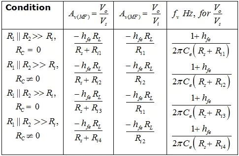
- Coupling capacitors (input and interstage) also affect the low-frequency response; their effect can be analysed using the effective input resistance R'i.
- The mid-band voltage gain of cascaded CE stages is the product of the individual stage gains, but current gain and overall input/output impedances must account for the loading effect of subsequent stages and bias resistors.
- Analysis of cascaded stages commonly proceeds from the last stage back to the input, evaluating Ai, Ri and Av stage by stage.
- For n identical cascaded stages, each with lower 3-dB frequency f1, the overall low-frequency 3-dB point f1(n) is given by the combination of individual high-pass responses and is typically higher (i.e. worse low-frequency response) than for a single stage.

- The amplifier's ability to handle a square wave is measured by sag. Sag depends on the lower 3-dB frequency f1 and the square-wave fundamental frequency f; smaller sag requires a lower f1.

- Transformer-coupled amplifiers designed for maximum power transfer typically have equal current and voltage gains under matched conditions. Their low-frequency response is limited by the transformer primary inductance Lp.

- To reproduce pulses of duration td with less than a specified sag, the transformer must have a minimum primary inductance.

High-Frequency Response of Amplifiers
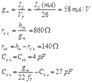
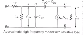
At high frequencies transistor internal capacitances and resistances become important. The hybrid-π model provides a convenient representation that includes junction capacitances and a base spreading resistance, which together produce frequency-dependent behaviour and the Miller effect.
- The high-frequency hybrid-π model parameters and the relations used to compute them are shown in the following figures and equations; numerical examples are often given for specific transistors (for example a 2N2218 silicon device).


 Notation and remarks:
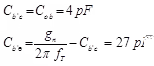
- Cb'c (often listed as Cob) is the collector-base capacitance measured with the emitter open.
- Cb'e is the base-emitter diffusion capacitance; it may be provided by the manufacturer or estimated from device parameters.
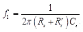
- fT is the transistor's unity-gain frequency: the frequency at which the short-circuit current gain in common-emitter configuration falls to unity. It is a key high-frequency figure-of-merit.
- The short-circuit current gain falls with frequency and is characterised by cut-off frequencies: α cut-off for common-base and β cut-off for common-emitter, each defined at the -3 dB point relative to mid-band.
- The gain-bandwidth product (GBW) is the product of mid-band gain and the bandwidth; for a transistor the unity-gain frequency fT is a common way to express GBW.
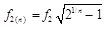
- For n cascaded identical CE stages, the overall high-frequency bandwidth is reduced; the combined bandwidth f2(overall) is determined by the cascade formula:
- The amplifier's rise time tr(for a step input or a square-wave leading edge) is approximately related to the bandwidth by:
- tr = 0.35 / f2
- When a transistor is driven into the high-frequency region with a resistive load, the collector-to-base capacitance appears amplified at the input because of the Miller effect, increasing the effective input capacitance and reducing voltage and current gain compared with the ideal α and β cut-off predictions.
- The high-frequency response of transformer-coupled amplifiers is often limited by the transformer's leakage inductance and distributed capacitance, which can create series resonance and limit usable bandwidth.
- Transistor noise is commonly specified as a spot noise figure (NF) or as an average noise figure; typical practical values are in the range 0.5 to 5 dB, depending on source resistance, collector current and frequency.
Practical Considerations and Design Notes
- Design of an amplifier for a given frequency band requires attention to both low- and high-frequency reactive elements: coupling and bypass capacitors at the low end, and junction capacitances and stray capacitances at the high end.
- When cascading stages, check loading between stages and match impedances where necessary to preserve gain and bandwidth.
- Use bypass capacitors large enough to push f1 well below the lowest signal frequency of interest; use coupling capacitors sized so that their reactance at the lowest frequency is small compared with the input resistances they drive.
- At high frequencies minimise lead lengths and stray capacitances, use proper layout and, when required, select transistors with suitable fT and low parasitic capacitances.
- For transformer-coupled stages, ensure the transformer primary inductance supports the required low-frequency performance and that leakage inductance and inter-winding capacitances are acceptable for the intended bandwidth.
Summary
The frequency response of an amplifier is determined by reactive elements at low frequency (coupling and bypass capacitors, transformer inductances) and by device parasitics at high frequency (junction and stray capacitances, base resistance). The hybrid and hybrid-π models, together with h-parameters and fT, provide practical tools for analysing gain, input/output impedances and bandwidth. Proper component selection and stage interconnection are essential to meet design goals for gain, bandwidth and waveform fidelity.
FAQs on Frequency Response
| 1. What is the frequency response of an amplifier? |  |
| 2. Why is frequency response important in amplifier design? | |
| 3. How is frequency response measured in amplifiers? | |
| 4. What is the significance of the bandwidth in amplifier frequency response? | |
| 5. How can the frequency response of an amplifier be improved? | |


 | Explore Courses for Electronics and Communication Engineering (ECE) exam |
 | Get EduRev Notes directly in your Google search |