Junction Theory & Different Types of Diodes & Their Characteristics - 1 | Electronic Devices - Electronics and Communication Engineering (ECE) PDF Download

Semiconductor Diode Characteristic
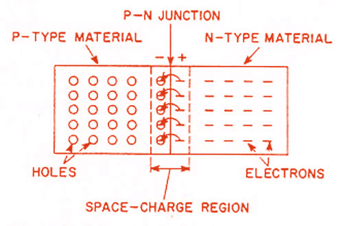
Formation of p-n Junctions
Semiconductor diodes are typically fabricated from silicon (Si) or germanium (Ge) crystals doped with specific impurities to create p-type or n-type regions. P-type material is formed by adding acceptor impurities (e.g., boron), while n-type material is created with donor impurities (e.g., phosphorus) during crystal growth. These crystals are sliced into thin wafers, which serve as the substrate for semiconductor devices.
P-n junctions are formed using several techniques:
- Alloying: A metal alloy is fused with the semiconductor to create a junction.
- Diffusion: Impurities are diffused into the wafer to form p- or n-type regions.
- Vapor Deposition (Epitaxial Growth): Thin layers of doped semiconductor are deposited on the wafer.
- Rate-Grown Junction: Controlled crystal growth introduces alternating p- and n-type regions.
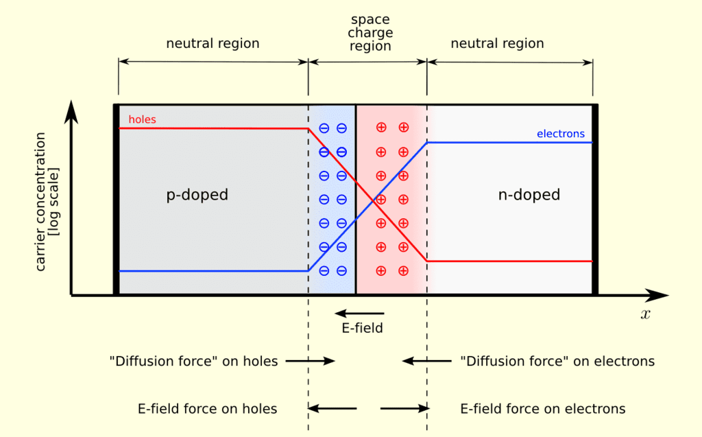
Charge Carriers and Junction Dynamics
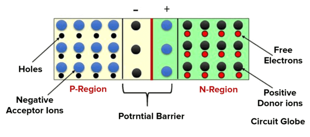
In a p-n junction, donor ions in the n-type region are represented by a positive charge (+), as they become positive ions after donating an electron. Acceptor ions in the p-type region are denoted by a negative charge (−), as they become negative ions after accepting an electron.
Initially, the p-type region (left of the junction) contains primarily holes, and the n-type region (right of the junction) contains primarily electrons. Due to the concentration gradient across the junction, holes diffuse from the p-side to the n-side, and electrons diffuse from the n-side to the p-side. This diffusion leaves behind unneutralized ions—positive donor ions on the n-side and negative acceptor ions on the p-side—forming a depletion region (also called the space-charge or transition region) near the junction. This region, depleted of mobile charge carriers, typically has a thickness of approximately 1 µm (10⁻⁶ m).
The diffusion of carriers creates an electric field across the depletion region, directed from the n-side to the p-side. This field opposes further diffusion, establishing equilibrium when the field strength balances the diffusion tendency. The resulting potential barrier, or contact potential (V₀), is typically a few tenths of a volt and prevents further net carrier movement.
Charge and Potential Distribution
The charge distribution, electric field, and potential across the junction are illustrated as follows:
- Charge Distribution: The depletion region contains unneutralized positive ions on the n-side and negative ions on the p-side.
- Electric Field: The field intensity peaks at the junction and decreases outside the depletion region.
- Electrostatic Potential: The potential varies across the depletion region, forming a barrier that inhibits further diffusion of holes and electrons.
- Potential Energy Barrier: This barrier opposes electron flow from the n-side to the p-side and hole flow from the p-side to the n-side .
The width of the depletion layer and the height of the potential barrier depend on the doping concentrations of the p- and n-type regions. Higher doping reduces the depletion width and increases the barrier height.
Equilibrium Conditions
At equilibrium, no net current flows across the p-n junction. The diffusion current (due to carrier concentration gradients) is exactly balanced by the drift current (due to the electric field). For holes and electrons, this balance is expressed as:
- = 0
- = 0
Thus, the drift and diffusion current densities components cancel each other for both carrier types.
Electrostatic Equations
The potential distribution in the junction satisfies the Poisson equation inside the depletion region:
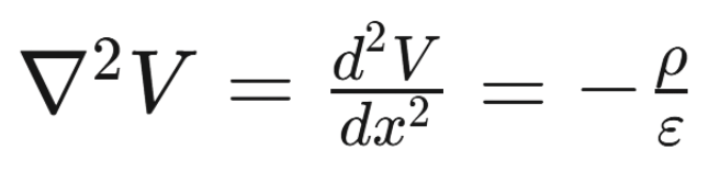
where is the charge density and is the permittivity of the semiconductor.
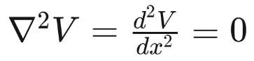
Outside the depletion region, where the charge density is zero, the potential satisfies the Laplace equation:
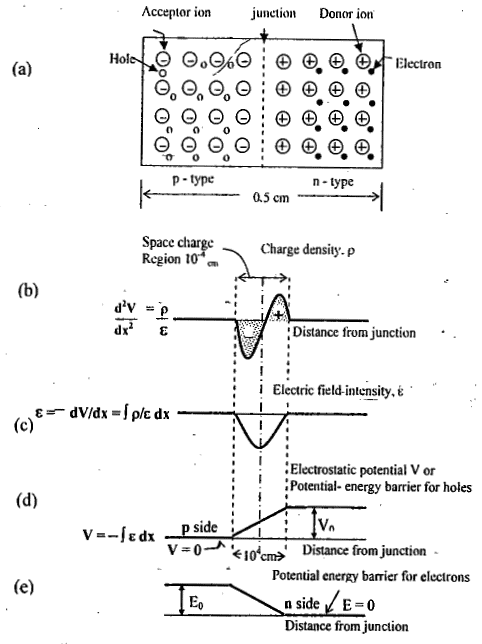 A schematic diagram of a p - n junction, including the charge density, electric field intensity, and potential - energy barriers at the junctions, (not drawn to scale.)
The P-N Junction as a Diode
Diode permits the easy flow of current in one direction but restrains the flow in die opposite direction.
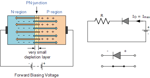
Forward Bias:
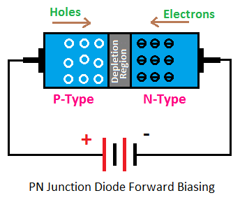
- Suppose we apply a voltage V such that n-side is negative and p-side is positive.
- The applied voltage V (or bias V) is opposite to the junction barrier potential V
- The consequences of this are:
(i) The effective barrier potential becomes (Vo — V) and hence the energy barrier across the junction decreases.
(ii) more majority carriers will be allowed to flow across the junction.
(iii) the junction width decreases. - The current flow is principally due to majority charge carriers and is large (mA).
Reverse Bias:
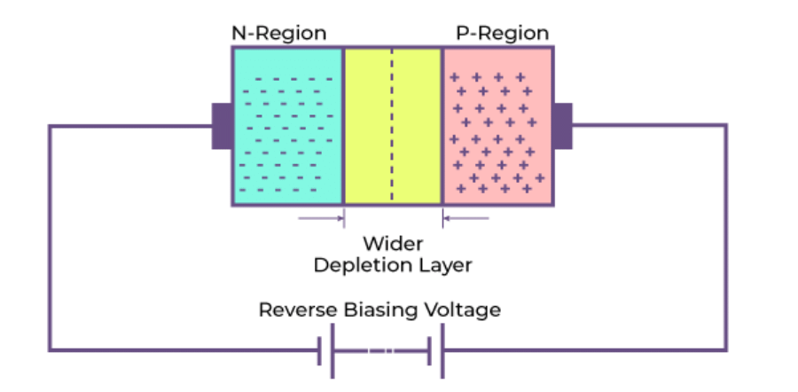
The applied voltage V on the n-side is positive and is negative on the p-side.
The applied bias V and the barrier potential V# are in the same direction making the effective junction potential as V + Vo. As a result, the junction width will increase.
The higher junction potential would restrict the flow of majority carriers to a much greater extent.
However, such a field will favour the flow of minority carriers (as they have opposite charges).
So, the reverse bias current will be due to the minority carriers only.
Since, the number of minority carriers is very small as compared to the majority carriers, the reverse bias current is small (≈ μA).
The short-circuited and open-circuited P-N Junction
- If the voltage V applied to the p-n junction is set equal to zero, the p-n junction would be short-circuited.
- Under this condition, no current can flow (I = 0) and the electrostatic potential Vo remains uncharged and equal to the value under open circuit conditions.
- The sum of the voltages around the closed loop must be zero, the junction potential V0 must be exactly compensated by the metal to semiconductor contact potentials at the ohmic contacts.
- It is not possible to measure contact difference of potential directly with a voltmeter across an open-circuited p-n junction diode and the voltmeter would read zero voltage.
Band AND Structure Of An Open-Circuited PN Junction
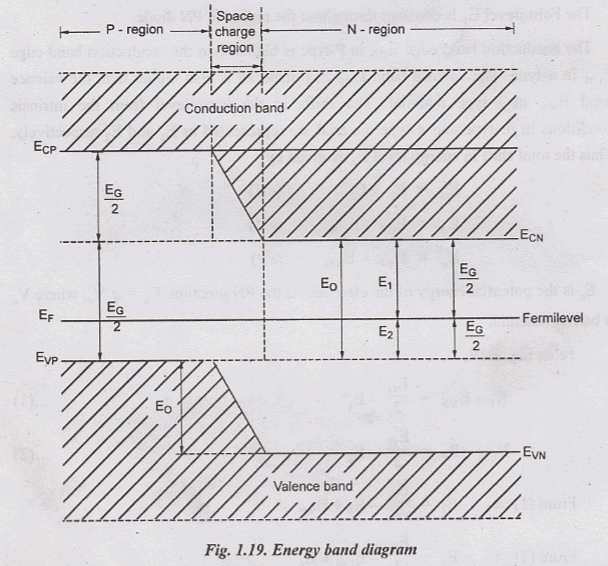
- The Fermi level must be constant throughout the specimen at equilibrium.
- The Fermi level EF is closer to the conduction band edge Ecn in the n-type material and closer to the valence band edge Evp in the p-side.
- The conduction band edge Ecp in the p material cannot be at the same level as Ecn, nor can the valence band edge Evn in the n-side line up with Evp. Hence the energy bandagram for a p-n junction appears as shown in fig.2 Where a shift in energy levels E0 is indicated. Note that
E0 = Ecp - Ecn = Evp - Evn = E1 + E2
This energy E0 represents the potential energy of the electrons at junction.
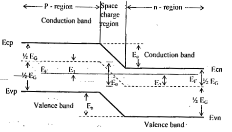 Band diagram for a p-n junction under open-circuit conditions. This sketch corresponds to fig (le) and represents potential energy for electrons. The width of the forbidden gap is Eg in electron volts.From figure,
EF - Evp - 1/2 EG - E1 and ECn - EF - 1/2 EG - E2 EG = forbidden energy gap
By adding the above equations
E0 = E1 + E2 = EG - (ECn - EF) - (EF - EVp)
EG = kT In |(NCNv) / ni2] ....(1)
Ecn - EF = kT ln (NC/ND) ....(2) ∴ KT = 26 meV
EF - Evp = kT ln (Nv/NA) ....(3)
The E’s are expressed in electron volts and-k has the dimensions of electron volts per degree Kelvin. The Contact difference in potential V0 is expressed in volts and is numerically equal to E0 and it is depends only upon the equilibrium concentrations, and not at all upon the charge density in the transition region(space charge region).
Other expressions for E0 are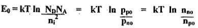 ....(4)
Rewriting the above equation (4) in another form
pp0 = pn0 ev0/vT
nn0 = np0 ev0/vT ....(5)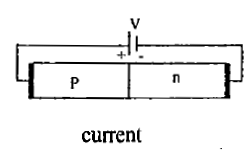
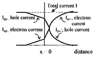
The hole and electron-current components vs, distance in a p-n junction diode. The space-charge region at the junction is assumed to be negligibly email
The Current Components in p-n Diode
- When a forward bias is applied to a diode, holes are injected into the n-side and electrons into the p-side.
- The number of these injected minority carriers falls off exponentially with distance from the junction as shown in fig.(3)
- The symbol Ipn(x) represents the hole current in the n material, and Inp(x) indicates the electron current in the p-side as a function of x.
- Electrons crossing the junction at x = 0 from right to left constitute a current in the same direction as holes crossing the junction from left to right. Hence the total current I at x = 0 is I = Ipn(0) + Inp(0)
- Consequently, in the p-side, there must be a second component of current Ipp which, when added to Iup, gives.the total current I. Hence this hole current in the p-side Ipp(a majority carrier current) is given by Ipp(x) = I - Inp(x)
- This current is plotted as a function of distance as shown in fig.(3) as is also the corresponding electron current lnn in the n material.
- For an un symmetrically doped diode, Ipn ≠ Inp.
- The current in a p-n diode is bipolar in character since it is made up of both positive and negative carriers of electricity.
- The total current is constant throughout the device, but the proportion due to holes and that due to electrons varies with distance.
Quantitative Theory of the P-N diode Currents
If the forward bias is applied to the diode, holes are injected from the p side into the n material. The concentration pn of holes in the n-side is increased above its thermal equilibrium value pno and, is given byPn(x) = Pno + Pn(0)e-x/Lp ....(6)
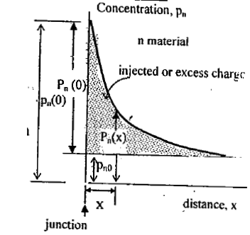
Defining the several components of hole concentration in the n side of a forward - biased diode.
Where the parameter Lp is called the diffusion length for holes in the n material.
And the injected or excess concentration at x = 0 is
Pn(0) = Pn(0) - Pno
The diffusion hole current in the n-side is given by
junction
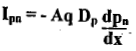 ....(7)
Taking the derivative of equation (6) and substituting in equation (7) we obtain
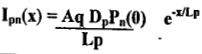 .... (8)
This equation verifies that the hole current decreases exponentially with distance.
Where q = charge of an electron
The Law of the Junction
- If the barrier potential across the depletion layer is VB, then
Pp = PnevB/VT ....(9)
This is the Boltzmann relationship of kinetic gas theory. - If we apply above equation to the case of an open-circuited p-n junction, then
Pp = Ppo, Pn = Pn0 and VB = V0. - Consider now a junction biased in the forward direction by an applied voltage V.
- Then the barrier voltage VB is decreased from its equilibrium value V0 by the amount or
Vb = V0 - V
V0 = equilibrium value - At the edge of the depletion layer, x = 0, pn = pn(0), then the above equation(9) is
Pp0 = Pn(0)e(V0 -V/Vt] ....(10)
Combining this equation with the above said equation(5), i.e., pp0 = pn0 eV0/VT
We obtain,
Pn(0) = Pn0ev/vT ....(11) - This boundary condition is called the “law of the junction”. It indicates that, for a forward bias (V > 0), the hole concentration pn(0) at the junction is greater than the thermal - equilibrium value pn0.
- A similar equation, valid for electrons, is obtained by interchanging p and n itt above equation( II).
- The hole concentration Pn(0) injected into the n side at the junction is given by
Pn(0) = Pn0(eV/VT-1) ....(12)
The Forward Currents
- The hole current Ipn(0) crossing the junction into the n-side at x = 0 is given by
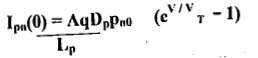
- The electron current Inp(0) crossing the junction into the p-side is obtained from above equation by interchanging n and p, or
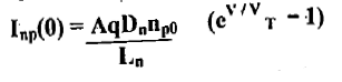
The total diode current I is the sum of Ipn(0) and Inp(0), or
I = I0(CV/VT -1)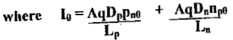
Hence I0 is called the "‘reverse saturation current!’ and depends on doping concentration.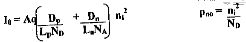
Where, σn = NDμnq and σp = NAμpq
VGO is a voltage which is numerically equal to the forbidden gap energy in electron volts. If we consider the recombination of carriers, then the total current I
I = I0(ev/nVT -1) ....(13)
Where η ≈ 2 for small (rated) currents and η ≈ 1 for large currents.
η ≅ 2 for silicon
η ≅ 1 for germanium - I0 depends on material and it is fixed for a given device. But varies with temperature
Io2 = I01 x 2I(T2 - T1)10l ....(14) - Where Io1 (I02) is the reverse saturation current at a temperature T1 (T2).
- I0 doubles for every 10°C rise in temperature. That is, it increases 7% / °C.
- I0 is in the range of microamperes for a germanium diode andTVano amperes for a silicon diode.
- Since n = 2 for small currents in silicon, the current increases as ev/2vT for the first several tenths of a volt and increases as ev/vT only at higher voltages.
The Volt-Ampere Characteristic
For a p-n junction, the current I is related to the voltage V by the equation
I = I0(ev/ηvT -1) ....(13)
η ≅ 1 for Ge
η ≅ 2 for Si
VT = T/11,600 = 26 m V at T = 300°K.
At room temperature,
(a) When the voltage V is positive and several times VT , the unity in the parenthesis of equation (13) may be neglected, i.e., ev/ηvT >>1,
∴ l = l0 ev/ηv T
Accordingly except for a small range in the neighborhood of the origin, the current increases exponentially with voltage.
(b) When the diode is reverse-biased and |V| is several times VT, I ≈ - I0. The “reverse
current” is therefore constant, independent of the applied reverse bias. Consequently, I0 is referred to as the “reverse saturation current”
At a reverse biasing voltage Vz, the diode characteristic exhibits an abrupt and marked departure from (13). At this critical voltage a large reverse current flows, and the diode is said to be in the “break down region”.
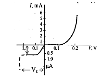 The volt-ampere characteristic for a germanium diode
The Cutin Voltage, Offset, break-point, or threshold voltage (Vy):
Below Vy the current is very small (say, less than 1 per cent of max. rated voltage).
Beyond Vy the current rises very rapidly. Vy = 0.2 V for Ge, 0.6 V for Si.
The reverse saturation current 10 in a Ge is normally larger by a factor of about 1000 than the 10 in a silicon diode of comparable ratings. Since n = 2 for small currents in Si, the 1 increases as eV/2VT only at higher voltages.
The resistance R, cutin voltage Vy, power dissipation and noise margin of Germanium is less— than the silicon. But Germanium is not used in switching characteristics.
The temperature dependence of p-n diode characteristics:
The dependence of 10 on temperature T is given approximately by
I0 = kTm e-v Go/ηvT
Where k is a constant and qVGO (q is the magnitude of the electron charge) is the forbidden gap energy in Joules:
For Ge : n = 1 m = 2 VGO = 0.785V
For Si: n = 2 m = 1.5 VGO = 1.21V
Taking the derivative of the logarithm of above equation, we find
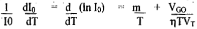
At room temperature, d(lnl0)/dT = 0.08 /°C for Silicon and 0.11 / °C for Germanium.
The 10 increases approximately 7 percent / °C for both Si and Ge. Since (1.07)10 ≈ 2.0, we conclude that the “reverse saturation current(Io)” approximately doubles for every 10°C rise in temperature.
Consider a diode operating at room temperature (300°K) and just beyond the Vy.
Then we find,
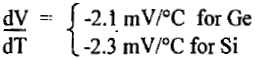
Since these data are based on “average characteristics”, it might be well for conservative design to assume a value of
dV / dT = -2.5 mV/°C ....(14)
for either Ge or Si at room temperature.
For Germanium, an increase in temperature from room temperature (25°C) to 90°C increases the 10 to hundreds of microamperes, although in Silicon at 100°C the 10 has increased only to some tenths of a micro ampere.
|
43 docs|29 tests
|
FAQs on Junction Theory & Different Types of Diodes & Their Characteristics - 1 - Electronic Devices - Electronics and Communication Engineering (ECE)
| 1. What is junction theory in electronics? |  |
| 2. What are diodes and what are their characteristics? | |
| 3. What are the different types of diodes? | |
| 4. How does a diode work? | |
| 5. What are the applications of diodes? | |


Summary
,Viva Questions
,past year papers
,MCQs
,Semester Notes
,video lectures
,Junction Theory & Different Types of Diodes & Their Characteristics - 1 | Electronic Devices - Electronics and Communication Engineering (ECE)
,Objective type Questions
,ppt
,Free
,practice quizzes
,Junction Theory & Different Types of Diodes & Their Characteristics - 1 | Electronic Devices - Electronics and Communication Engineering (ECE)
,Important questions
,shortcuts and tricks
,Previous Year Questions with Solutions
,Exam
,study material
,Sample Paper
,Junction Theory & Different Types of Diodes & Their Characteristics - 1 | Electronic Devices - Electronics and Communication Engineering (ECE)
,Extra Questions
,mock tests for examination
;


Junction Theory & Different Types of Diodes & Their Characteristics - 1 Free PDF Download
Importance of Junction Theory & Different Types of Diodes & Their Characteristics - 1
Junction Theory & Different Types of Diodes & Their Characteristics - 1 Notes
Junction Theory & Different Types of Diodes & Their Characteristics - 1 Electronics and Communication Engineering (ECE) Questions
Study Junction Theory & Different Types of Diodes & Their Characteristics - 1 on the App
|
© EduRev
|
Education Revolution
|


|


