Study Notes: Amplifiers


Multistage Amplifier
For many practical systems a single-transistor amplifier cannot provide the required overall gain, input/output impedance matching or bandwidth. A practical solution is to combine two or more amplifier stages so that the output of one stage becomes the input of the next. This arrangement is commonly called cascading.
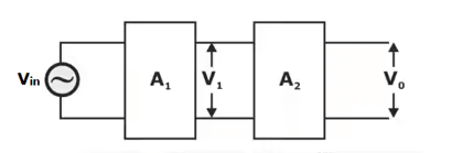 Figure 1
When stages are cascaded, the overall voltage gain is the product of the individual stage voltage gains.

Here,
- AV = overall voltage gain
- AV1 = voltage gain of first stage
- AV2 = voltage gain of second stage
Note: For n cascaded stages the overall voltage gain is the product of the n individual stage gains.
Effect of Cascading on Bandwidth
Cascading affects the frequency response of the overall amplifier. In general, cascading single-pole (first-order) stages reduces the overall bandwidth; the combined -3 dB points shift from those of a single stage. The quantitative effect depends on whether stages are identical or not.
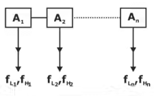
Identical stages
For n identical first-order stages, each having the same lower cutoff frequency fL and upper cutoff frequency fH, the combined response is the product of the individual responses. For the upper cutoff (high-cut) the overall -3 dB frequency f'H is obtained by solving
$ (1 + (ω/ω_H)²)^{n/2} $ = $ \sqrt{2} $
which yields
$ ω'_H $= $ωH · \sqrt{(2^{\frac{1}{n}} - 1})$
or
$ f'_H = f_H · √(2^{1/n} - 1) $
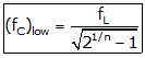
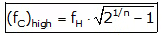
Similarly, for cascaded identical high-pass stages the overall lower cutoff frequency f'L moves according to the same factor (reciprocal where appropriate). Thus the overall bandwidth is reduced compared with a single stage. The overall bandwidth is
BW' = f'H - f'L
Non-identical stages
When stages have different single-stage bandwidths, each contributes its own pole and zero to the overall response; the -3 dB points must be found from the magnitude of the product of the individual transfer functions. The dominant pole (the pole closest to the passband) usually determines the overall bandwidth.
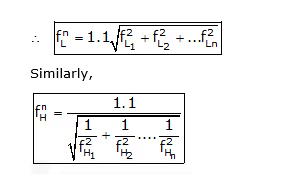
Types of Coupling and Comparison
Between cascaded stages a coupling network is used so that minimum signal loss occurs while blocking the DC bias of one stage from disturbing the next stage. The common coupling methods are:
- RC coupling
- Transformer coupling
- Direct (DC) coupling
Brief comparison (qualitative):
- RC coupling - simple, low cost, good for audio and mid-frequency amplifiers, but the coupling capacitor and input resistance introduce low-frequency roll-off.
- Transformer coupling - allows impedance matching and efficient power transfer at a desired frequency, increases low-frequency performance for a given load, but transformers are bulky, expensive and frequency-limited.
- Direct coupling - no coupling capacitor or transformer; useful when amplifying signals down to DC, but DC bias levels must be carefully arranged so stages do not disturb each other.
Popular Cascading Designs
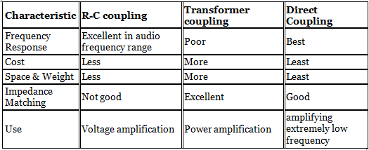
Cascade (Cascode) Amplifier: CE-CB configuration
The cascode amplifier combines a common-emitter (CE) stage followed by a common-base (CB) stage. The CB stage is inherently wideband because its grounded base shields the input from Miller feedback from the collector, so the cascode gives improved high-frequency response compared with a single CE stage.
Key points:
- The CE input stage provides moderate input impedance (kΩs) and drives the low input-impedance CB stage.
- The common-base stage is not subject to Miller feedback because the base is at AC ground; hence the high-frequency roll-off caused by the collector-base capacitance is much reduced.
- To keep the CE stage gain low (reducing any Miller effect), the load seen by the CE stage can be made small (for example, the emitter resistance of the CB stage loading the CE collector). If the CE stage voltage gain is ≈ 1 then the Miller capacitance CMiller ≈ CCBO (1 - AV) ≈ 2CCBO for AV ≈ -1.
- The overall cascode has high voltage gain, moderately high input impedance, high output impedance and significantly increased bandwidth compared with a single CE stage.
The total current gain of an ideal cascode is ≈ β (the current gain of the CE stage is ≈ 1 while that of the CB stage is ≈ β).
Note: A cascode amplifier offers a useful trade-off: wide bandwidth without the severe Miller effect that limits a single CE amplifier at high frequencies.
Darlington Pair (CC-CC)
A Darlington pair is two emitter-followers cascaded so that the emitter of the first device drives the base of the second. The overall voltage gain is close to unity, but the input impedance is very high and the output impedance is very low.
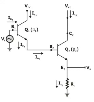
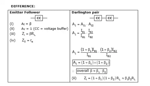
Important characteristics:
- Extremely high input impedance
- Very large current gain (approximately the product of the two transistor β values)
- Very low output impedance
Feedback Amplifier
A feedback amplifier contains a path from output back to input that returns a portion of the output signal to the input. The fraction of output returned is called the feedback factor (β). If the returned signal opposes the input signal the feedback is negative; if it adds to the input signal the feedback is positive.
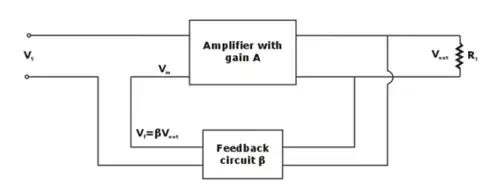 Figure 5: Basic Feedback Amplifier
Positive vs Negative Feedback
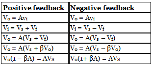
In block-diagram terms the closed-loop gain with feedback is
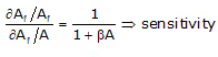
Af = A / (1 ± Aβ)
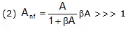
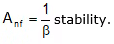
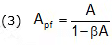
where the sign is negative for negative feedback and positive for positive feedback. For negative feedback the closed-loop gain is reduced (Anf < A), while for positive feedback the closed-loop gain can be larger and may lead to instability (oscillation) if Aβ → 1.
Concluding inequality often quoted:
Apf > A > Anf
Note: Negative feedback is widely used to stabilise amplifiers and improve linearity; positive feedback is used in oscillators and regenerative circuits.
Effects of Negative Feedback
Negative feedback, when applied appropriately, produces several useful effects:
- Improved stability and reduced sensitivity of the closed-loop gain to component variations and temperature
- Increase (or decrease) of input impedance depending on the feedback topology
- Decrease (or increase) of output impedance depending on the topology
- Improved linearity and reduction of distortion
- Increase in bandwidth (trade-off with closed-loop gain)
Stability / desensitivity
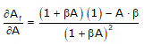
If the open-loop gain A changes by a small fractional amount then the fractional change in closed-loop gain with negative feedback is reduced roughly by the factor 1/(1 + Aβ). Thus the closed-loop gain is less sensitive to variations in A when Aβ is large.

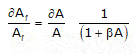
Note: Increased desensitivity means the amplifier is less sensitive to temperature, device ageing and other perturbations.
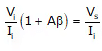
Increase in input impedance (voltage-series feedback)
For voltage-series (series mixing, voltage sampling) negative feedback the input sees the returned signal in series with the input; therefore the input impedance increases approximately by the factor (1 + Aβ):
Vi = Vs - Vf
Vi = Vs - βV0
Vi = Vs - βA Vi
Vi (1 + Aβ) = Vs
Therefore Zi,with feedback = Zi(1 + Aβ)
Decrease in output impedance (voltage feedback)
For many voltage-feedback topologies the output impedance is reduced by the factor (1 + Aβ):
V0 + βA V0 = I0 Z0

Increase in bandwidth
Negative feedback tends to widen the amplifier bandwidth at the expense of closed-loop gain. Approximately, for a single dominant pole, the new lower and upper cutoff frequencies scale as:
f'L ≈ fL / (1 + Aβ)
f'H ≈ (1 + Aβ) fH
Hence the closed-loop bandwidth BW' ≈ BW · (1 + Aβ) when Aβ ≫ 1.
Types of Negative Feedback Amplifier
Negative feedback circuits are classified according to the quantity sampled at the output (voltage or current) and the way the feedback signal is returned to the input (series or shunt). The four main types are:
- Voltage-series feedback - a fraction of output voltage is returned in series with the input. Input impedance increases and output impedance decreases. (Diagram below shows series connection at input and voltage sampling at output.)
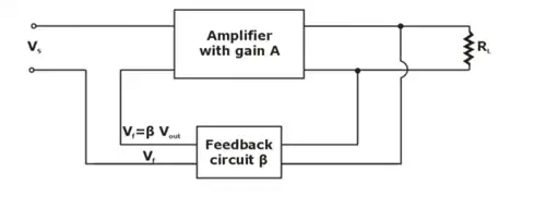 Figure 6: Voltage Series Feedback
- Voltage-shunt feedback - a fraction of output voltage is returned in shunt (parallel) with the input. Input impedance decreases and output impedance decreases.
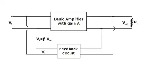 Figure 7: Voltage Shunt Feedback
- Current-series feedback - a fraction of output current is returned in series with the input. Input impedance increases and output impedance increases.
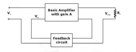 Figure 8: Current Series Feedback
- Current-shunt feedback - a fraction of output current is returned in shunt with the input. Input impedance decreases and output impedance increases.
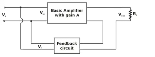 Figure 9: Current Shunt Feedback
Basics of Power Amplifier
- An amplifier is an electronic device that increases the magnitude of voltage, current or power of an input signal by using an external power source.
- A power amplifier increases the power level of a signal and is typically used in the final stage of audio and radio transmitters where significant power must be delivered to a load (speaker, antenna, etc.).
Classification based on Mode of Operation
Power amplifiers are classified by the fraction of the input cycle during which the device conducts (conduction angle). Common classes are:
- Class A
- Class B
- Class AB
- Class C
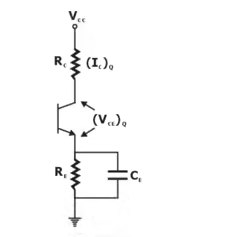
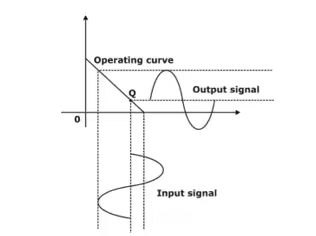
Class A Power Amplifier
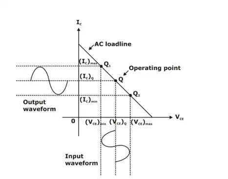
In a class A amplifier the device conducts for the entire 360° of the input cycle. The operating point Q is set so that the transistor remains in its linear region for the full cycle. A transformer is often used at the collector (or output) to provide impedance matching to the load and to allow the load to see the required AC voltage swing.
DC power drawn from the supply VCC is
Pin = VCC · ICQ
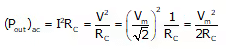
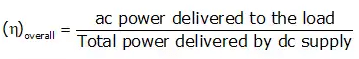
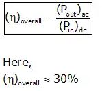
The AC power delivered to the load depends on the output peak voltage Vm and RMS current. The overall efficiency η is defined as the ratio of AC output power to DC input power. For a single-ended transformer-coupled Class A amplifier the theoretical maximum efficiency is 50% under ideal sinusoidal conditions.
Disadvantages: low efficiency and significant power dissipation in the device.
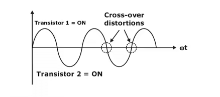
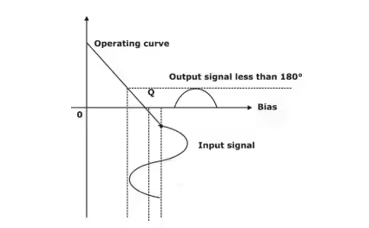
Class B Power Amplifier
In a class B amplifier each device conducts for half the input cycle (180°). A single transistor amplifies only the positive (or negative) half cycle, so distortion occurs if a single transistor is used. To overcome this, class B is commonly implemented in a push-pull pair where one device conducts on the positive half and the other on the negative half. Push-pull reduces even-order distortion and improves efficiency compared with class A.
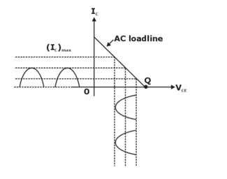
In push-pull class B, the waveforms and the RMS values of currents and voltages determine the output power and the DC power drawn. For an ideal class B push-pull stage with sinusoidal drive, the theoretical maximum efficiency is π/4 ≈ 0.785 or 78.5%.
Power efficiency derivation for class B push-pull (summary steps)
The following lines give the essential steps in the standard derivation for ideal class B push-pull efficiency:
I = peak output current
RMS value of collector (output) current = I / √2
RMS value of output voltage = (I · RL) / √2
AC output power = (Vrms · Irms) = (I² RL) / 2
DC input power from supplies (average over cycle for two devices) = (2·VCC·Iavg,each) and for the ideal sinusoidal case this evaluates so that
Maximum theoretical efficiency = π/4 ≈ 78.5%


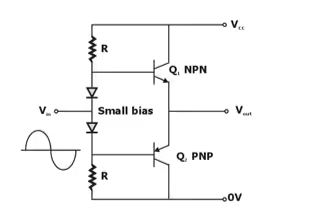
Class AB Power Amplifier
Class AB operation is an intermediate between class A and class B. Each device conducts for slightly more than half the cycle (conduction angle between 180° and 360°). This reduces the crossover distortion present in pure class B while giving improved efficiency over class A. The efficiency depends on the bias and conduction angle and typically lies between about 50% and 70% under practical conditions.
Class C Power Amplifier
In class C operation the device conducts for significantly less than 180° of the input cycle. Class C amplifiers are highly efficient but severely non-linear and are therefore used where the output is filtered by a resonant tuned circuit (for example, RF transmitters) so that the required sinusoidal output is reconstructed by the tank circuit. Conduction angle is less than 180° and efficiency can be high, but linearity is poor.
FAQs on Study Notes: Amplifiers
| 1. What is the effect of cascading on the bandwidth of a multistage amplifier? |  |
| 2. What are the types of coupling used in multistage amplifiers and how do they compare? | |
| 3. What is a popular cascading design used in multistage amplifiers? | |
| 4. What is the power efficiency of a CLASS B push-pull amplifier? | |
| 5. What are the basics of a power amplifier? | |


 | Explore Courses for Electronics and Communication Engineering (ECE) exam |
 | Get EduRev Notes directly in your Google search |