Physics Exam  >  Physics Notes  >  Solid State Physics, Devices & Electronics  >  Origin of Energy Bands

Origin of Energy Bands | Solid State Physics, Devices & Electronics PDF Download

Origin of Energy Bands


The failure of the free electron model is due to the over simplified assumption that a conduction electron in a metal experiences a constant or zero potential due to the ion cores and hence is free to move about crystal.
Now the periodic potential described below forms the basis of the band Theory of solids. The behavior of an electron in this potential is describe by constructing the electron wave functions using one-electron approximates.
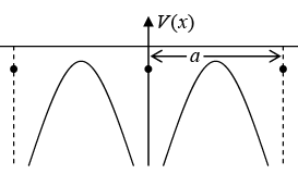
Origin of Energy Bands | Solid State Physics, Devices & Electronics

As we shall discuss later, the motion of an electron in a periodic potential yields the following results.
(a) There exist allowed energy bands separated by forbidden region or band gap.
(b) The electronic energy function E(K) is periodic in the wave vector K
In the free electron Theory E varies with K  

Origin of Energy Bands | Solid State Physics, Devices & Electronics

The Block Theorem


The 1-D Schrödinger equation for an electron moving in a constant potential V0 is  
Origin of Energy Bands | Solid State Physics, Devices & Electronics The solution ψ(x) = e±ikx
For periodic potential with period equal to the lattice constant a we have
ψ(x) = e±ikx Uk(x)    where Uk = Uk (x + a)  
Note: Let g(x) and f(x) be two real and independent solution to the second order differential The general equation can be written as   ψ(x) = A f(x) + B g(x)
while Origin of Energy Bands | Solid State Physics, Devices & Electronics  = constant
In three dimensions, the block Theorem is expressed as  
Origin of Energy Bands | Solid State Physics, Devices & Electronics
Thus the wave function becomes the one of a free electron. 

The Kronig-Penney Model 

This model illustrates the behaviour of electrons in a periodic potential by assuming a relatively simple one-dimensional model of periodic potential as shown figure.
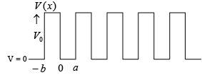
Origin of Energy Bands | Solid State Physics, Devices & Electronics

For this potential write down the Schrödinger wave equation and its general solution with taking potential constant finally. We get
Origin of Energy Bands | Solid State Physics, Devices & Electronics
which is a measure of the area V0b of the potential barrier. Thus increasing P has the physical meaning of bonding an electron more strongly to a particular potential well
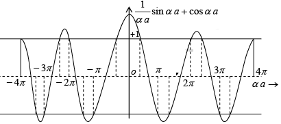
Origin of Energy Bands | Solid State Physics, Devices & Electronics 

We know that Origin of Energy Bands | Solid State Physics, Devices & Electronics

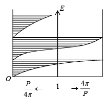
It may be noted that since α2 is proportional to the energy E the abscissa is a measure of the energy. The following conclusion may be drawn from figure.
(i) The energy spectrum of the electrons consists of alternate regions of allowed energy bands (solid lines on abscissa) and forbidden energy band (broken lines)
(ii) The width of the allowed energy bands increases with αa or the energy
(iii) The width of  particular allowed energy band decreases with increase in  value of P.

Figure- Allowed (shaded) and forbidden (open) energy ranges as a function of P
Origin of Energy Bands | Solid State Physics, Devices & Electronics

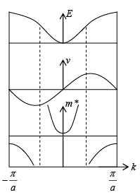
 Energy Verses Wave-Vector relationship
The energy E is also an even periodic function of k with period of 2π/a i.e k = ± nπ/a
dn = (1/2π)dk
Velocity is Origin of Energy Bands | Solid State Physics, Devices & Electronics

Concept Effective Mass and Holes  

In one dimension, an electron with wave-vector k has group velocity  
Origin of Energy Bands | Solid State Physics, Devices & Electronics ...(i)
If an electric field ε acts on the electron, then in time δ t . It will do work  
δ E = force times distance= −eε vδ t  (ii)  
But   Origin of Energy Bands | Solid State Physics, Devices & Electronics (iii)
So, comparing equation (ii) with (iii), we have  
 Origin of Energy Bands | Solid State Physics, Devices & Electronics(iv)
In terms of force F, Origin of Energy Bands | Solid State Physics, Devices & Electronics
Generalising to three dimensions: Origin of Energy Bands | Solid State Physics, Devices & Electronics
Origin of Energy Bands | Solid State Physics, Devices & Electronics

where Origin of Energy Bands | Solid State Physics, Devices & Electronics
From equation (i) v Origin of Energy Bands | Solid State Physics, Devices & Electronics
Differentiating with respect to time Origin of Energy Bands | Solid State Physics, Devices & Electronics

But from equation (iv), Origin of Energy Bands | Solid State Physics, Devices & Electronics
 SoOrigin of Energy Bands | Solid State Physics, Devices & Electronics
But from Newton’s equation we expect Origin of Energy Bands | Solid State Physics, Devices & Electronics
which leads us to define an effective mass Origin of Energy Bands | Solid State Physics, Devices & Electronics
That is  
The dynamics of electrons is modified by the crystal potential;  
The effective mass depends on the curvature of the bands;  
Flat bands have large effective ma      
Near the bottom of a band, m* is positive, near the top of a band, m* is negative.  

Hole Concept 

➤ Hole wavevector: The total k of a full band is zero: if we remove an electron with wavevector ke the total k of the band is  kh +ke = 0⇒ kh = −ke
➤ Hole energy: Take the energy zero to be the top of the valence band. The lower the electron energy, the more energy it takes to remove it; thus
Eh(kh) = -Ee(ke)
But bands are usually symmetric, E(k) =E (−k)
So Eh(kh) = Eh(-kh) = -Ee(ke)
➤ Hole velocity: In three dimensions Origin of Energy Bands | Solid State Physics, Devices & Electronics
But kh =−ke So  Origin of Energy Bands | Solid State Physics, Devices & Electronics
and so   Origin of Energy Bands | Solid State Physics, Devices & Electronics
The group velocity of the hole is the same as that of the electron.  

➤ Hole effective mass: The curvature of E is just the negative of the curvature of − E ,  
So mh* = −me*
Note that this has the pleasant effect that if the electron effective mass is negative, as it is at the top of the band, the equivalent hole has a positive effective mass.  

➤ Hole dynamics
We know that Origin of Energy Bands | Solid State Physics, Devices & Electronics
Substituting kh =−ke and vh = ve gives  
Origin of Energy Bands | Solid State Physics, Devices & Electronics
Exactly the equation of motion for a particle of positive charge.  
Under an electric field, electrons and holes acquire drift velocities in opposite directions, but both give electric current in the direction of the field.  

The document Origin of Energy Bands | Solid State Physics, Devices & Electronics is a part of the Physics Course Solid State Physics, Devices & Electronics.
All you need of Physics at this link: Physics
91 videos|21 docs|25 tests

FAQs on Origin of Energy Bands - Solid State Physics, Devices & Electronics

1. What is the origin of energy bands in materials?
Ans. The origin of energy bands in materials is due to the arrangement of electrons in atoms and their interactions with neighboring atoms. When atoms come together to form a solid, their orbitals overlap, leading to the formation of molecular orbitals. These molecular orbitals extend over the entire crystal lattice, and the energy levels of these extended orbitals form energy bands.
2. How do energy bands determine the electrical properties of materials?
Ans. The energy bands in materials determine their electrical properties by defining the energy levels at which electrons can exist. The valence band contains electrons that are tightly bound to atoms and do not contribute to electrical conduction. On the other hand, the conduction band contains vacant or loosely bound states where electrons can move freely and contribute to electrical conduction. The energy gap between the valence and conduction bands determines whether a material is an insulator, semiconductor, or conductor.
3. What is the significance of energy band structure in semiconductors?
Ans. The energy band structure in semiconductors is of significant importance as it determines the electrical conductivity and optical properties of these materials. Semiconductors have a small energy gap between the valence and conduction bands, allowing electrons to move from the valence band to the conduction band with the application of a small amount of energy. This property makes semiconductors suitable for various electronic and optoelectronic devices.
4. How are energy bands experimentally studied in materials?
Ans. Energy bands in materials can be experimentally studied using techniques such as photoemission spectroscopy, tunneling spectroscopy, and angle-resolved photoemission spectroscopy. These techniques involve the measurement of the energy and momentum of electrons in the material, providing information about the band structure and electronic properties.
5. Can the energy band structure of a material be modified?
Ans. Yes, the energy band structure of a material can be modified through various means. For example, doping impurities into a semiconductor can introduce energy levels in the band gap, altering the conductivity of the material. Applying external electric or magnetic fields can also modify the band structure by shifting energy levels or splitting bands. Additionally, the band structure can be engineered through the design and synthesis of materials with specific compositions and structures.
91 videos|21 docs|25 tests
Download as PDF
Explore Courses for Physics exam
Signup for Free!
Signup to see your scores go up within 7 days! Learn & Practice with 1000+ FREE Notes, Videos & Tests.
10M+ students study on EduRev
Related Searches

Viva Questions

,

Devices & Electronics

,

Previous Year Questions with Solutions

,

Origin of Energy Bands | Solid State Physics

,

Devices & Electronics

,

past year papers

,

Origin of Energy Bands | Solid State Physics

,

Semester Notes

,

Sample Paper

,

shortcuts and tricks

,

video lectures

,

Origin of Energy Bands | Solid State Physics

,

MCQs

,

study material

,

Extra Questions

,

Free

,

ppt

,

Important questions

,

practice quizzes

,

Objective type Questions

,

mock tests for examination

,

pdf

,

Summary

,

Devices & Electronics

,

Exam

;