Operational Amplifier | Solid State Physics, Devices & Electronics PDF Download
Characteristics of an Op-Amp
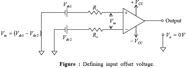
➤ Input Offset Voltage
Input offset voltage is the voltage that must be applied between the two input terminals of an op-amp to null the output, as shown in figure. In the figure Vdc1 and Vdc2 are dc voltages and Rs represent the source resistance.
➤ Input Offset Current
The algebraic difference between the currents into the inverting and non-inverting terminal is referred to as input offset current Iio . Thus Iio = IB1 − IB2 where IB1 is the current into the non-inverting input and IB2 is the current into the inverting input. As the matching between two input terminals is improved, the difference between IB1 and IB2 becomes smaller; that is the Iio value decreases further. 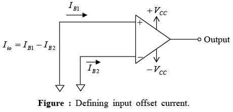
➤ Input Bias Current
Input bias current IB is the average of the currents that flow into the inverting and noninverting input terminals of the op-amp. In equation form 
➤Differential Input Resistance
Differential input resistance Ri (often referred to as input resistance) is the equivalent resistance that can be measured at either the inverting or non-inverting input terminal with the other terminal connected to ground.
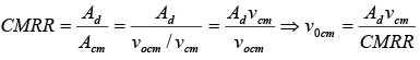
➤Common-mode Rejection Ratio (CMRR)
- The common-mode rejection ratio (CMRR) is defined as the ratio of the differential voltage gain Ad to the common-mode voltage gain Acm ; that is, CMRR = Ad/Acm.
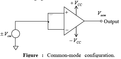
- The differential voltage gain Ad is the same as the large-signal voltage gain A , which is specified on the data sheets; however, the common-mode voltage gain can be determined from the circuit shown in figure and using the equation Acm = Vocm/Vcm
where Vocm = output common-mode voltage, Vcm = input common-mode voltage, Acm = common-mode voltage gain.
- The CMRR can also be expressed as the ratio of the change in input offset voltage to the total change in common-mode voltage. Thus CMRR = Vio/vcm. Thus
 .
. - The CMRR value is very large and is therefore usually specified in decibels (dB). Thus CMRR(dB) =
 or CMRR(dB) =
 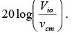 Generally Acm is very small and Ad = A is very large; therefore, the CMRR is very large. The higher the value of CMRR, the better is the matching between two input terminals and the smaller is the output common-mode voltage.
➤ Supply Voltage Rejection Ratio
- The change in an op-amp’s input offset voltage Vio caused by variations in supply voltages is called the supply voltage rejection ratio (SVRR).
- A variety of terms equivalent to SVRR are used by different manufacturers. Such as the power supply rejection ratio (PSRR) and the power supply sensitivity (PSS). These terms are expressed either in microvolt per volt or in decibels.
- If we denote the change in supply voltages by ΔV , SVRR can be defined as follows:
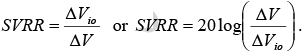
This means that the lower the value of SVRR in microvolt/volt, the better for op-amp performance.
➤ Large-signal Voltage Gain
Since the op-amp amplifies difference voltage between two input terminals, the voltage gain of the amplifier is defined as: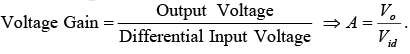
Because output signal amplitude is much larger than the input signal, the voltage gain is commonly called large-signal voltage gain.
➤ Output Voltage Swing
The output voltage swing Vo max of the Op-Amp is guaranteed to be between +VCC and -VCC. In fact, the output voltage swing indicates the values of positive and negative saturation voltages of the op-amp. The output voltage never exceeds these limits for given supply voltages +VCC and −VCC .
➤ Output Resistance
Output resistance Ro is the equivalent resistance that can be measured between the output terminal of the op-amp and the ground.
➤ Transient Response
- The response of any practically useful network to a given input is composed of two parts: the transient and steady-state response. The transient response is that portion of the complete response before the output attains some fixed value.
- Once reached, this fixed value remains at that level and is, therefore, referred to as a steady-state value. The response of the network after it attains a fixed value is independent of time and is called the steady-state response.
- Unlike the steady-state response, the transient response is time variant. The rise time and the percent of overshoot are the characteristics of the transient response. The time required by the output to go from 10% to 90% of its final value is called the rise time.
- Conversely, overshoot is the maximum amount by which the output deviates from the steady-state value. Overshoot is generally expressed as a percentage. Smaller the value of rise time larger is the bandwidth.
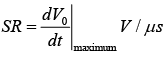
➤ Slew Rate
- Slew rate (SR) is defined as the maximum rate of change of output voltage per unit of time and is expressed in volts per microseconds.
 .
. - Slew rate indicates how rapidly the output of an op-amp can change in response to changes in the input frequency. The slew rate changes with change in voltage gain and is normally specified at unity (+1) gain.
- The slew rate of an op-amp is fixed; therefore, if the slope requirements of the output signal are greater than the slew rate, then distortion occurs.
- Thus slew rate is one of the important factors in selecting the op-amp for ac applications, particularly at relatively high frequencies.
➤ Gain-Bandwidth Product
The gain-bandwidth product (GB) is the bandwidth of the op-amp when the voltage gain is 1. Equivalent terms for gain-bandwidth product are closed-loop bandwidth, unity gain bandwidth, and small-signal bandwidth.
➤The Ideal Op-Amp
An ideal op-amp would exhibit the following electrical characteristics:
- Infinite voltage gain A .
- Infinite input resistance Ri so that almost any signal source can drive it and there is no loading of the preceding stage.
- Zero output resistance Ro so that output can drive an infinite number of other devices.
- Zero output voltage when input voltage is zero.
- Infinite bandwidth so that any frequency signal from 0 to ∞ Hz can be amplified without attenuation.
- Infinite common-mode rejection ratio so that the output common-mode noise voltage is zero.
- Infinite slew rate so that output voltage changes occur simultaneously with input voltage changes.
There are practical op-amps that can be made to approximate some of these characteristics using a negative feedback arrangement. In particular, the input resistance, output resistance, and bandwidth can be brought close to ideal values by this method.
➤Equivalent Circuit of an Op-Amp
- Figure shows an equivalent circuit of an op-amp. This circuit includes important values from the data sheets: A , Ri and Ro . Note that Avid is an equivalent Thevenin voltage source, and Ro is the Thevenin equivalent resistance looking back into the output terminal of an op-amp.
- The equivalent circuit is useful in analyzing the basic operating principles of op-amps and in observing the effects of feedback arrangements. For the circuit shown, the output voltage is: v0 = Avid = A(v1-v2)
where A = large-signal voltage gain, vid = difference input voltage
v1 = voltage at the non-inverting input terminal with respect to ground
v2 = voltage at the inverting terminal with respect to ground.
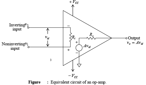
- Equation v0 = Avid = A(v1-v2) indicates that the output voltage v0 is directly proportional to the algebraic difference between the two input voltages. In other words, the op-amp amplifies the difference between the two input voltages; it does not amplify the input voltages themselves. For this reason the polarity of the output voltage depends on the polarity of the difference voltage.
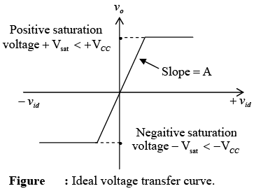
➤ Ideal Voltage Transfer Curve
Equation v0 = Avid = A(v1-v2) is the basic op-amp equation, in which the output offset voltage is assumed to be zero. This equation is useful in studying the op-amp’s characteristics and in analyzing different circuit configurations that employ feedback. The graphic representation of this equation is shown in figure, where the output voltage v0 is plotted against input difference voltage vid keeping gain A constant.
Open-Loop Op-Amp Configurations
In the case of amplifiers the term open loop indicates that no connection, either direct or via another network, exists between the output and input terminals. That is, the output signal is not fed back in any form as part of the input signal, and the loop that would have been formed with feedback is open.
When connected in open-loop configuration, the op-amp simply functions as a high-gain amplifier. There are three open-loop op-amp configurations:
1. Differential amplifier
2. Inverting amplifier
3. Non-inverting amplifier
These configurations are classed according to the number of inputs used and the terminal to which the input is applied when a single input is used.
➤ The Differential Amplifier
Figure shows the open-loop differential amplifier in which input signals vin1 and vin2 are applied to the positive and negative input terminals. Since the op-amp amplifies the difference between the two input signals, this configuration is called the differential amplifier. The op-amp is a versatile device because it amplifies both ac and dc voltages. The source resistances Rin1 and Rin2 are normally negligible compared to the input resistance Ri . Therefore, the voltage drops across these resistors can be assumed to be zero, which then implies that v1 = vin1 and v2 = vin2 thus v0 = A(vin1 - vin2).
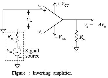
➤The inverting Amplifier
- In the inverting amplifier only one input is applied and that is to the inverting input terminal. The non-inverting input terminal is grounded as shown in figure. ∵v1 = 0V and v2 = vin thus v0= - Avin.
- The negative sign indicates that the output voltage is out of phase with respect to input by 1800 or is of opposite polarity. Thus in the inverting amplifier the input signal is amplified by gain A and is also inverted at the output.
➤The Non-inverting Amplifier
- Figure shows the open-loop non-inverting amplifier. In this configuration the input is applied to the non-inverting input terminal, and the inverting terminal is connected to ground.
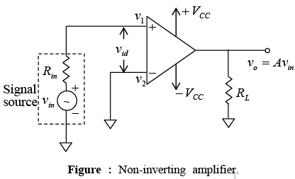
- In the circuit, v1 = vin and v2 = 0V, thus vo = Avin. This means that the output voltage is larger than the input voltage by gain A and is in phase with the input signal. In all three open-loop configurations any input signal (differential or single) that is only slightly greater than zero drives the output to saturation level. This results from the very high gain (A) of the op-amp.
NOTE: Thus, when operated open-loop, the output of the op-amp is either negative or positive saturation or switches between positive and negative saturation levels. For this reason, open-loop op-amp configurations are not used in linear applications.
An Op-Amp with Negative Feedback
- The open-loop gain of an operational amplifier (op-amp) is very high, which means it can amplify small signals (around microvolts or less) effectively. However, these small signals are very sensitive to noise and are difficult to measure accurately in a lab setting.
- Additionally, the open-loop voltage gain of an op-amp is not a constant value. It can vary due to changes in temperature and power supply, making it unsuitable for many linear applications. In these applications, the output should be proportional to the input and of the same type.
- Moreover, the bandwidth of most open-loop op-amps is very small, nearly zero. This limitation makes them impractical for AC applications.
- By modifying the basic circuit, we can select and control the gain of the op-amp. This modification involves using feedback, where an output signal is sent back to the input either directly or through another network.
- If the feedback signal is of the opposite polarity or out of phase by 180 degrees (or odd multiples of 180 degrees) with respect to the input signal, it is known as negative feedback. An amplifier with negative feedback can self-correct for any changes in output voltage caused by environmental conditions.
- If the feedback signal is in phase with the input signal, it is called positive feedback. This type of feedback enhances the input signal and is also known as regenerative feedback. Positive feedback is essential in oscillator circuits.
- Using negative feedback in amplifiers helps to stabilize the gain, increase the bandwidth, and alter the input and output resistances. However, this improvement comes at the cost of a reduced voltage gain.
- Other advantages of negative feedback include a decrease in harmonic or nonlinear distortion and a reduction in the effect of input offset voltage at the output. It also lessens the impact of changes in temperature and supply voltages on the op-amp's output.
➤ Block Diagram Representation of Feedback Configurations
- An operational amplifier (op-amp) that utilizes feedback is known as a feedback amplifier.
- This type of amplifier is often called a closed-loop amplifier because the feedback creates a closed loop between its input and output.
- A feedback amplifier is made up of two main parts:
- The op-amp
- The feedback circuit
- The feedback circuit can have various designs depending on what the amplifier is meant to do.
- This feedback circuit can include:
- Passive components
- Active components
- Combinations of both types
- To explain the basic ideas of feedback, we will focus only on purely resistive feedback circuits.
- A closed-loop amplifier can be shown with two blocks:
- One block represents the op-amp
- The other block represents the feedback circuit
- There are four ways to connect these two blocks, based on whether the feedback is voltage or current and how it is fed back:
- Voltage-series feedback
- Voltage-shunt feedback
- Current-series feedback
- Current-shunt feedback
- The four configurations are illustrated in a figure.
- In the figures labeled (a) and (b):
- The voltage across the load resistor RL serves as the input voltage to the feedback circuit.
- The feedback quantity (either voltage or current) comes from the feedback circuit and is proportional to the output voltage.
- In the current-series and current-shunt feedback circuits shown in figures (c) and (d):
- The load current iL flows into the feedback circuit.
- The output from the feedback circuit (whether voltage or current) is proportional to the load current iL.
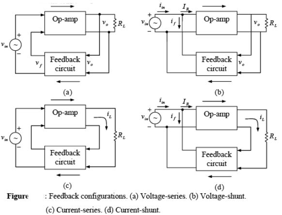
The voltage-series and voltage-shunt feedback configurations are important because they are most commonly used. An in-depth analysis of these two configurations is presented here, computing voltage gain, input resistance, output resistance and bandwidth for each.

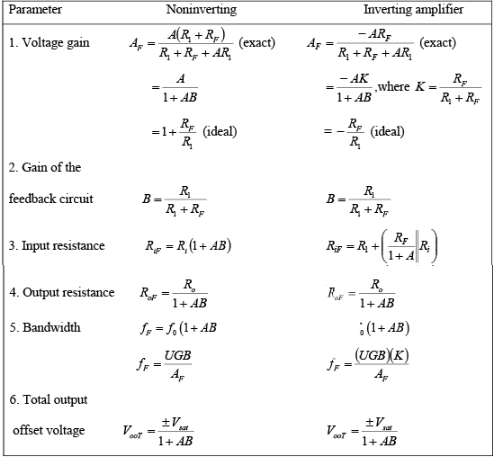
Voltage-Series Feedback Amplifier (Non-inverting feedback Amp)
The schematic diagram of the voltage-series feedback amplifier is shown in figure. The op-amp is represented by its schematic symbol, including its large-signal voltage gain A and the feedback of two resistors R1 and RF. The voltage gain for the op-amp with and without feedback, and the gain of the feedback circuit are defined as follows:
Open-loop voltage gain (or gain without feedback) A = v0/vid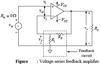
Closed-loop voltage gain (or gain with feedback) AF = v0/vin
Gain of the feedback circuit = B = vf/v0
➤ Negative Feedback
- Kirchhoff's voltage law for the input loop can be expressed as: vid = vin - vf
- In this equation:
- vin represents the input voltage.
- vf is the feedback voltage.
- vid is the difference input voltage.
- The difference voltage vid is calculated by taking the input voltage vin and subtracting the feedback voltage vf.
- This means that the feedback voltage vf always works against the input voltage vin.
- As a result, the feedback voltage is considered to be negative because it is out of phase with the input voltage by 180 degrees.
➤Closed-Loop Voltage Gain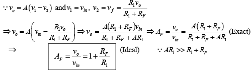
The above equation is important because it shows that the gain of the voltage-series feedback amplifier is determined by the ratio of two resistors, R1 and RF .
As defined previously, the gain of the feedback circuit (B) is the ratio of vf and vo. Thus 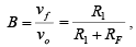 we can conclude that AF = 1/B(ideal)
This means that the gain of the feedback circuit is the reciprocal of the closed-loop voltage gain. In other words for given R1 and RF the values of AF and B are fixed. Finally, the closed-loop voltage gain AF can be expressed in terms of open-loop gain A and feedback circuit gain B as follows. Thus 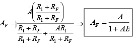 where AB = loop gain.
➤ Difference Input Voltage Ideally Zero
∵ vid = v0/A ⇒ vid ≅ 0 ⇒ v1 ≅ v2 (Since A is very large (ideally infinite))
That is the voltage at the noninverting input terminal of an op-amp is approximately equal to that at the inverting input terminal provided that A is very large. This concept is useful in the analysis of closed-loop op-amp circuits.
For example, ideal closed-loop voltage gain can be obtained using the preceding results as follows. In the circuit of voltage series feedback amplifier, 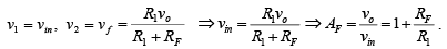
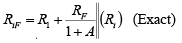
➤ Input Resistance with Feedback
Let Ri is the input resistance (open-loop) of the op-amp, and RiF is the input resistance of the amplifier with feedback. Then RiF = Ri (1+AB)
This means that the input resistance of the op-amp with feedback is (1 + AB) times that without feedback.
➤ Output Resistance with Feedback
Output resistance is the resistance determined looking back into the feedback amplifier from the output terminal. Thus RoF = Ro/1+AB
The result shows that the output resistance of the voltage-series feedback amplifier is 1/ (1 + AB) times the output resistance Ro of the op-amp. That is, the output resistance of the op-amp with feedback is much smaller than the output resistance without feedback.
➤ Bandwidth with Feedback
The bandwidth of an amplifier is defined as the band (range) of frequencies for which the gain remains constant. fF = f0(1+AB) of the noninverting amplifier with feedback, fF is equal to its bandwidth without feedback, f0 times (1 + AB).
➤ Total Output Offset Voltage with Feedback
In an open-loop op-amp the total output offset voltage is equal to either the positive or negative saturation voltage. Since with feedback the gain of the non-inverting amplifier changes from A to A / (1 + AB) the total output offset voltage with feedback must also be 1/ (1 + AB) times the voltage without feedback. That is  From this analysis it is clear that the non-inverting amplifier with feedback exhibits the characteristics of the perfect voltage amplifier. That is, it has very high input resistance, very low output resistance, stable voltage gain, large bandwidth, and very little (ideally zero) output offset voltage.
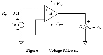
➤ Voltage Follower
The lowest gain that can be obtained from a non-inverting amplifier with feedback is 1. When the non-inverting amplifier is configured for unity gain, it is called a voltage follower because the output voltage is equal to and in phase with the input. In other words, in the voltage follower the output follows the input.
Although it is similar to the discrete emitter follower, the voltage follower is preferred because it has much higher input resistance, and the output amplitude is exactly equal to the input.
To obtain the voltage follower from the non-inverting amplifier simply open R1 and short RF. The resulting circuit is shown in figure. In this figure all the output voltage is fed back into the inverting terminal of the op-amp; consequently, the gain of the feedback circuit is 1 ( B =AF= 1).
 Thus
Thus 
The voltage follower is also called a non-inverting buffer because, when placed between two networks, it removes the loading on the first network.
Voltage-Shunt Feedback Amplifier (Inverting Amplifier with Feedback)
Figure shows the voltage shunt feedback amplifier using an op-amp. Note that the non-inverting terminal is grounded, and the feedback circuit has only one resistor RF. However, an extra resistor R1 is connected in series with the input signal source vin.
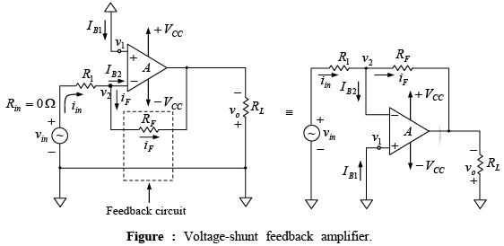
➤ Closed-Loop Voltage Gain
The closed-loop voltage gain AF of the voltage-shunt feedback amplifier can be obtained by writing Kirchhoff’s current equation at the input node v2 as follows: iin =iF + IB Since Ri is very large, the input bias current IB is negligibly small.
Therefore 
The negative sign in equation indicates that the input and output signals are out of phase by 180o (or of opposite polarities). In fact, because of this phase inversion, the configuration is commonly called an inverting amplifier with feedback.
This equation shows that the gain of the inverting amplifier is set by selecting a ratio of feedback resistance RF to the input resistance R1. In fact, the ratios RF/R1 can be set to any value whatsoever, even to less than 1. Because of this property of the gain equation, the inverting amplifier configuration with feedback lends itself to a majority of applications as against those of the non-inverting amplifier. where
where  is a voltage attenuation factor,
  is gain of the feedback circuit.
➤ Inverting Input Terminal at Virtual Ground
The difference input voltage is ideally zero; that is, the voltage at the inverting terminal (v2) is approximately equal to that at the non-inverting terminal (v1). In other words, the inverting terminal voltage v2 is approximately at ground potential. Therefore, the inverting terminal is said to be at virtual ground. This concept is extremely useful in the analysis of closed-loop inverting amplifier circuits. For example, ideal closed-loop gain can be obtained using the virtual-ground concept as follows: 
➤Input Resistance with Feedback
Since Ri and A are very large 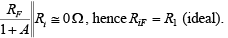
➤Output Resistance with Feedback
RoF = R0/1+AB
➤Bandwidth with Feedback
fF = f0(1+AB)
where f0 = break frequency of the op-amp 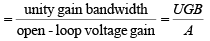
Thus 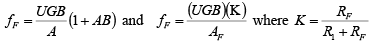 and
and 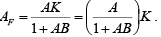
➤Total Output Offset Voltage with Feedback
(Total Output Offset Voltage with Feedback) = total output offset voltage without feedback/1+AB
i.e. 
➤Current-to-Voltage Converter
Let us reconsider the ideal voltage-gain equation of the inverting amplifier, 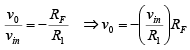
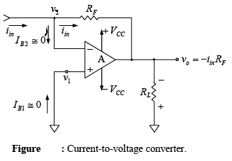
However, since v1 = 0V and v1 = v2.
vin/R1 = iin and v0 = -iinRF.
This means that if we replace the vin and R1 combination by a current source iin as shown in figure, the output voltage vo becomes proportional to the input current iin. In other words, the circuit converts the input current into a proportional output voltage.
One of the most common uses of the current-to-voltage converter is in sensing current from photo detectors and in digital-to-analog converter applications.
Table: Summary of results obtained for non-inverting and inverting amplifiers
 |
OP–amp Nat Level – 1
|
Start Test |
Differential Amplifiers
➤ Differential Amplifier with One Op-Amp
Figure below shows the differential amplifier with one op-amp. A close examination of the differential amplifier is a combination of inverting and non-inverting amplifier.
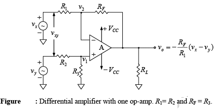 When vy = 0V, the configuration becomes an inverting amplifier; hence the output due
to vx only is vox = -(RF(vx)/R1)
Similarly, when vx = 0V, the configuration is a non-inverting amplifier having a voltage divider network composed of R2 and R3 at the non-inverting input.
Therefore,  and the output due to vy then is voy =
Thus the net output voltage is 
Note that the gain of the differential amplifier is the same as that of the inverting amplifier.
➤Differential Amplifier with Two Op-Amps
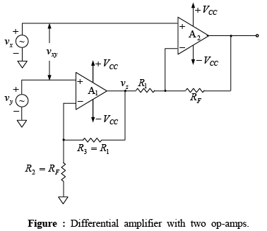
The output vz of the first stage is 
By applying the superposition theorem to the second stage, we can obtain the output
voltage: 
Since R1 = R3 and RF = R2, v0 = -
Therefore, 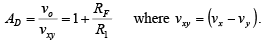
The Practical Op-Amp
Offset minimizing resistance  is used in non-inverting and inverting configuration as shown in figure given below.
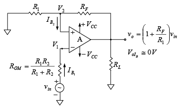 Figure : Non-inverting amplifier with offset minimizing resistor ROM.
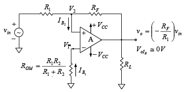 Figure : Inverting amplifier with offset minimizing resistor ROM.
Summing, Scaling and Averaging Amplifier
This section shows how the inverting, non-inverting and differential configurations are useful in such applications as summing, scaling and averaging amplifiers.
➤ Inverting Configuration
Figure below shows the inverting configuration with three inputs Va , Vb and Vc . Depending on the relationship between the feedback resistor RF and the input resistors Ra, Rb and Rc the circuit can be used as a summing amplifier, scaling amplifier or averaging amplifier.
The circuit’s function can be verified by examining the expression for the output voltage
V0 which is obtained from Kirchhoff’s current equation written at node V2.
Ia+Ib+Ic = IB+IF
Since Ri and A of the op-amp are ideally infinity, IB = 0 A and V1 =V2 ≅ 0V.
Therefore, 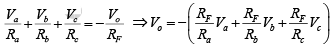
- Summing amplifier
If in the circuit, Ra = Rb= Rc = RF then V0 = -(Va + Vb + Vc) hence the circuit is called summing amplifier. - Scaling or weighted amplifier
If each input voltage is amplified by a different factor, in other words, weighted differently at the output, the circuit is then called a scaling or weighted amplifier. This condition can be accomplished if Ra , Rb and Rc are different in value. Thus the output voltage of the scaling amplifier is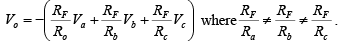
- Average circuit
The circuit can be used as an averaging circuit, in which the output voltage is equal to the average of all the input voltages. This is accomplished by using all input resistors of equal value Ra = Rb = Rc = R . In addition, the gain by which each input is amplified must be equal to 1 over the number of inputs; that is, RF/R = 1/n where n is the number of inputs. Thus, if there are three inputs, we want RF/R = 1/3, consequently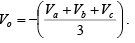
➤ Non-inverting Configuration
If input voltage sources and resistors are connected to the non-inverting terminal as shown in figure below, the circuit can be used either as a summing or averaging amplifier through selection of appropriate values of resistors, that is, R1 and RF.
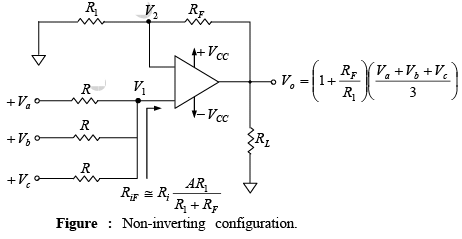
Again, to verify the functions of the circuit, the expression for the output voltage must be obtained. Recall that the input resistance RiF is very large. Therefore, using the superposition theorem, the voltage V1 at the non-inverting terminal is 
- Averaging amplifier
Above equation shows that the output voltage is equal to the average of all input voltages times the gain of the circuit (1 + (RF/R1)), hence the name averaging amplifier. Depending on the application gain is 1 (RF = 0) the output voltage will be equal to the average of all input voltages.
Summing amplifier If 1 + (RF/R1)=3, then RF = 2R1 = Vo = Va + Vb + Vc
➤Differential Configuration (Subtractor)
A basic differential amplifier can be used as a subtractor as shown in figure below.
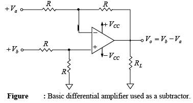 From this figure, the output voltage of the differential amplifier with a gain of 1 is
V0 = -(R/R)(Va-Vb)⇒V0 = Vb - Va
Summing amplifier
A four-input summing amplifier may be constructed using the basic differential amplifier if two additional input sources are connected, one each to the inverting and non-inverting input terminals through resistor R (as shown in figure). 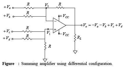 The output voltage equation for this circuit can be obtained by using the superposition theorem. For instance, to find the output voltage due to Va alone, reduce all other input voltages Vb , Vc and Vd to zero as shown in figure below.
 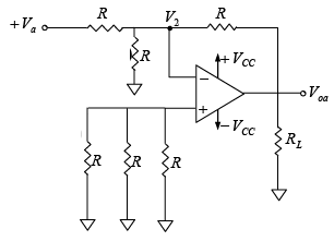 Figure : Deriving the output voltage equation from the summing amplifier. In fact, this circuit is an inverting amplifier in which the inverting input is at virtual ground (V2=0V) .
Therefore, the output voltage is Voa = -(R/R)Va= -Va.
Similarly, the output voltage due to Vb alone is Vob = −Vb.
Now if input voltages Va , Vb and Vc are set to zero, the circuit becomes a non-inverting amplifier in which the voltage V1 at the non-inverting input is 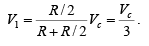
This means that the output voltage due to Vc alone is
Similarly, the output voltage due to all four input voltages is given by
Vo = Voa + Vab + Voc + Vod = −Va − Vb + Vc + Vd
Notice that the output voltage is equal to the sum of the input voltages applied to the noninverting terminal plus the negative sum of the input voltages applied to the inverting terminal.
The Integrator
A circuit in which the output voltage waveform is the integral of the input voltage waveform is the integrator or the integration amplifier. Such a circuit is obtained by using a basic inverting amplifier configuration if the feedback resistor RF is replaced by a capacitor CF (figure shown below)
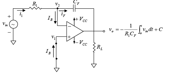 Figure (a): The integrator circuit.
The expression for the output voltage vo can be obtained by writing Kirchhoff’s current equation at node v2 : i1 =IB+ iF ⇒ i1≅iF (Since IB is negligibly small)
Recall that the relationship between current through and voltage across the capacitor is 
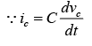
 ∵ v1 = v2 ≅ 0
The output voltage can be obtained by integrating both sides with respect to time: 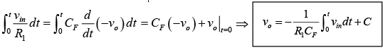
where C is the integration constant and is proportional to the value of the output voltage
vo at time t = 0 seconds.
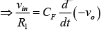
The waveforms are drawn with the assumption that R1CF = 1 second and VooT = 0V, that is, C = 0.  Figure (b): Input and ideal output waveforms using a sine wave and square wave, respectively. R1CF = 1 second and VooT = 0V assumed.
When vin= 0 the integrator works as an open-loop amplifier. This is because the capacitor CF acts as an open circuit  to the input offset voltage Vio. In other words, the input offset voltage Vio and the part of the input current charging capacitor CF produce the error voltage at the output of the integrator. Therefore, in the practical integrator shown in figure below, to reduce the error voltage at the output, a resistor RF limits the low-frequency gain and hence minimizes the variations in the output voltage.
 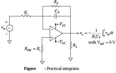 The frequency response of the basic integrator is shown in figure below.
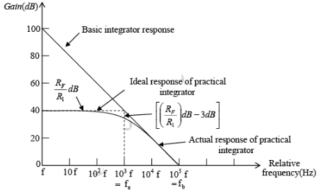
Figure : Frequency response of basic and practical integrators: 
In this figure fb is the frequency at which the gain is 0 dB and is given by 
The frequency response of the practical integrator is shown in the figure by a dashed line. In this figure, f is some relative operating frequency and for frequencies f to fa the gain RF / R1 is constant. However after f a gain decreases at a rate 20 dB / decade . In other words, between fa and fb the circuit acts as an integrator. The gain-limiting frequency fa is given by 
Generally, the value of fa and in turn R1CF and RFCF values should be selected such that fa < fb . For example if fa =fb /10 then RF = 10 R1. In fact, the input signal will be integrated properly if the time period T of the signal is larger than or equal to RFCF. That is, T ≥RFCF where 
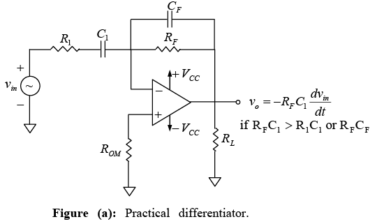
The Differentiator
Figure below shows the differentiator or differentiation amplifier. As its name implies, the circuit performs the mathematical operation of differentiation: that is the output waveform is the derivative of the input waveform. The differentiator may be constructed from a basic inverting amplifier if an input resistor R1 is replaced by capacitor C1.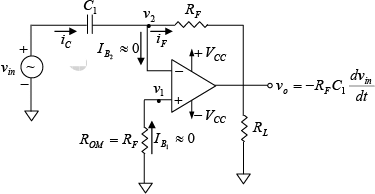 Figure : Basic differentiator Circuit.
The expression for the output voltage can be obtained from Kirchhoff’s current equation written at node v2 as follows: iC =IB + iF⇒ iC ≅ iF ∵ IB ≅ 0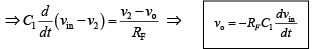
The gain of the circuit ( RF / XC1) increases with increase in frequency at a rate of 20 dB / decade . This makes the circuit unstable. Also, the input impedance  decreases with increase in frequency, which makes the circuit very susceptible to high frequency noise. When amplified, this noise can completely override the differentiated output signal. This frequency response of the basic differentiator is shown in figure below.
 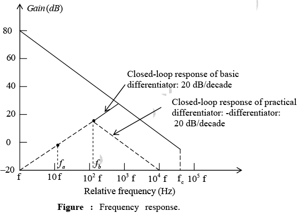 In this figure, fa is the frequency at which the gain is 0 dB and is given by
 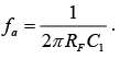 Both the stability and the high-frequency noise problems can be corrected by the addition of two components: R1 and CF as shown in figure below. This circuit is a practical differentiator.
 The frequency response is shown in figure by a dashed line. From frequency f to fb the gain increases at 20 dB / decade . However after fb the gain decreases at 20 dB / decade . This 40 dB / decade change in gain is caused by the R1C1 and RFCF combinations. The gain-limiting frequency fb is given by
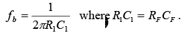
Thus, R1C1 and RFCF help to reduce significantly the effect of high-frequency input, amplifier noise, and offsets. Above all, it makes the circuit more stable by preventing the increase in gain with frequency. Generally, the value of fb and in turn R1C1 and RFCF values should be selected such that fa<fb
where 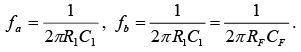
The input signal will be differentiated properly if the time period T of the input signal is larger than or equal to RFC1. That is, T ≥ RFC1.
Figure below show the sine wave and square wave inputs and resulting differentiated outputs, respectively, for the practical differentiator.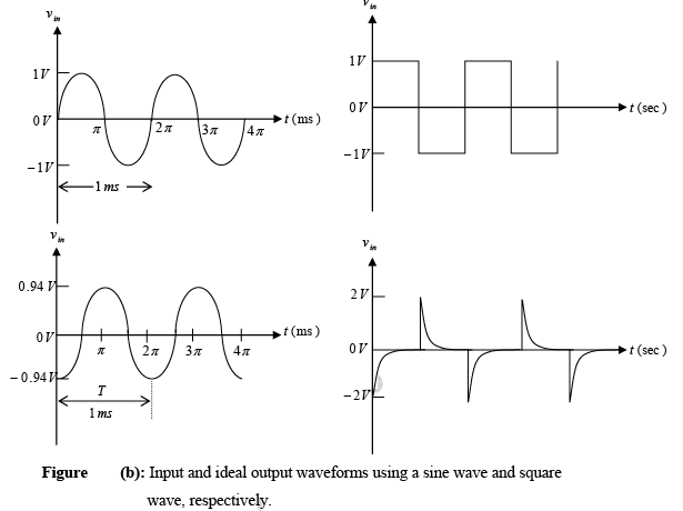 A workable differentiator can be designed by implementing the following steps:
- Select fa equal to the highest frequency of the input signal to be differentiated. Then, assuming a value of C1 < 1 μF , calculate the value of RF .
- Choose fb = 20 fa and calculate the values of R1 and CF so that R1C1 = RFCF.
The differentiator is most commonly used in wave shaping circuits to detect high frequency components in an input signal and also as a rate-of-change detector in FM modulators.
 |
Download the notes
Operational Amplifier
|
Download as PDF |
Active Filters
An electric filter is often a frequency-selective circuit that passes a specified band of frequencies and blocks or attenuates signals of frequencies outside this band. Filters may be classified in a number of ways:
1. Analog or digital
2. Passive or active
3. Audio (AF) or radio frequency (RF)
Analog filters are designed to process analog signals, while digital filters process analog signals using digital techniques. Depending on the type of elements used in their construction, filters may be classified as passive or active. Elements used in passive filters are resistors, capacitors, and inductors. Active filters, on the other hand employ transistors or op-amps in addition to the resistors and capacitors. The type of element used dictates the operating frequency range of the filter. For example, RC filters are commonly used for audio or low frequency operation, whereas LC or crystal filters are employed at RF or high frequencies.
An active filter offers the following advantages over a passive filter:
1. Gain and frequency adjustment flexibility. Since the op-amp is capable of providing a gain, the input signal is not attenuated as it is in a passive filter. In addition, the active filter is easier to tune or adjust.
2. No loading problem. Because of the high input resistance and low output resistance of the op-amp, the active filter does not cause loading of the source or load.
3. Cost. Typically, active filters are more economical than passive filters. This is because of the variety of cheaper op-amps and the absence of inductors.
The most commonly used filters are:
1. Low-Pass filter
2.High-Pass filter
3.Band-Pass filter
4. Band-Reject filters
5. All-Pass filter
All of these filters uses an op-amp as the active element and resistors and capacitors as the passive element. Figure below shows the frequency response characteristics of the five types of filters. The ideal response is shown by dashed curves, while the solid lines indicate the practical filter response. 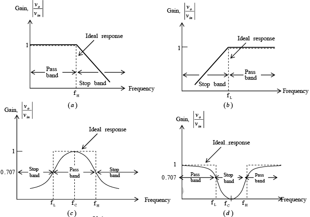
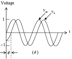 Figure : Frequency response of the major active filters.
(a) Low pass. (b) High pass. (c) Band pass. (d) Band rejects. (e) Phase shift between input and output volages of an all-pass filter.
➤First-Order Low-Pass Filter
Figure below shows a first-order low-pass Butterworth filter that uses an RC network for filtering. Note that the op-amp is used in the non-inverting configuration; hence it does not load down the RC network. Resistors R1 and RF determine the gain of the filter.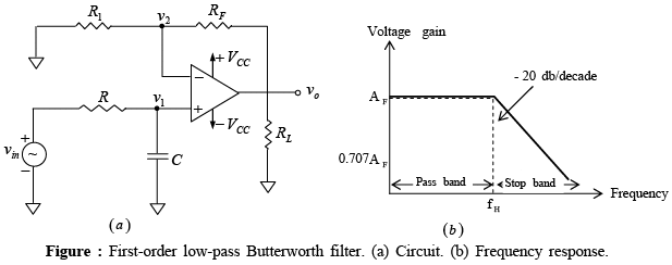
According to the voltage-divider rule, the voltage at the non-inverting terminal (across capacitor C) is 
On simplifying, we get  and the output voltage
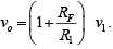
That is, 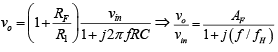
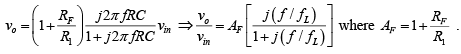
Where vo/vin = gain of the filter as a function of frequency, AF = 1 + (RF/R1) =
pass-band gain of the filter, f = frequency of the input signal and fH = 1/2πRC= high cutoff frequency of the filter.
The gain magnitude and phase angle equations of the low-pass filter can be obtained as follows: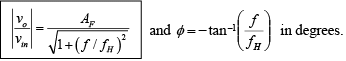
The operation of the low-pass filter can be verified from the gain magnitude equation:
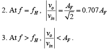
1. At very low frequencies, that is, 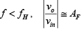
➤ Second-Order Low-Pass Filter
A stop-band response having a 40 dB / decade roll-off is obtained with the second-order low-pass filter. A first-order low-pass filter can be converted into a second-order type simply by using an additional RC network, as shown in figure below.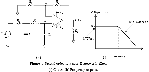
Second-order filters are important because higher-order filters can be designed using them. The gain of the second-order filter is set by R1 and RF while the high cutoff frequency fH is determined by R2 , C2 , R3 and C3 as follows: 
Furthermore, for a second-order low-pass Butterworth response, the voltage gain magnitude equation is: 
where  pass-band gain of the filter, f = frequency of the input signal (Hz)
➤ First-Order High-Pass Filter
A first-order high-pass filter is formed from a first-order low-pass type by interchanging components R and C. Figure below shows a first-order high-pass Butterworth filter with a low cutoff frequency of fL. This is the frequency at which the magnitude of the gain is 0.707 times its pass-band value. Obviously, all frequencies higher than fL are pass-band frequencies, with the highest frequency determined by the closed loop bandwidth of the op-amp.
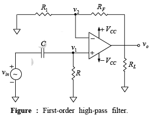
Hence the magnitude of the voltage gain is 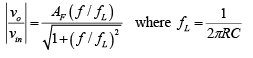
➤ Second-Order High-Pass Filter
As in the case of the first-order filter, a second-order high-pass filter can be formed from a second-order low-pass filter simply by interchanging the frequency determining resistors and capacitors. Figure below shows the second-order high-pass filter.
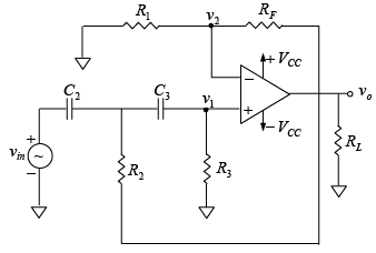 Figure : Second order high-pass Butterworth filter.
The voltage gain magnitude equation of the second-order high-pass filter is as follows: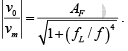
where AF = pass-band gain for the second-order Butterworth response, f = frequency of the input signal (Hz), fL = low cutoff frequency (Hz).
Since second-order low-pass and high-pass filters are the same circuits except that the positions of resistors and capacitors are interchanged, the design and frequency scaling procedures for the high-pass filter are the same as those for the low-pass filter.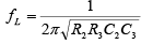
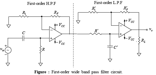
➤Band-Pass Filter
A wide band-pass filter can be formed by simply cascading high-pass and low-pass sections and is generally the choice for simplicity of design and performance. The order of the band-pass filter depends on the order of the high-pass and low-pass filter sections.
➤All-Pass Filter
As the name suggests, an all-pass filter passes all frequency components of the input signal without attenuation, while providing predictable phase shifts for different frequencies of the input signal.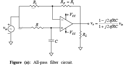 The output voltage vo of the filter can be obtained by using the superposition theorem.
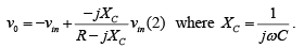
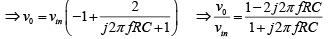
Above equation indicates that the amplitude of vo/vm is unity; that is, v0 =|vin| throughout the useful frequency range, and the phase shift between v0 and vin is a function of input frequency f the phase angle φ is given by 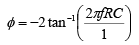
where φ is in degrees, f in hertz, R in ohms, and C in farads. This equation is used to find the phase angle φ if f , R, and C are known. Figure below shows a phased shift of 90o between the input vin and output v0 . That is v0 lags vin by 90o. For fixed values of R and C, the phase angle φ changes from 0 to -180o as the frequency f is varied from 0 to ∞. In all-pass filter circuit, if the positions of R and C are interchanged, the phase shift between input and output becomes positive. That is, output v0 leads input vin .
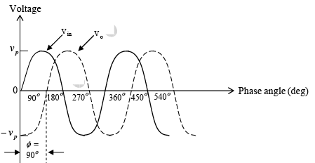 Figure (b): phase shift between input and output voltages.
Oscillators
Basically, the function of an oscillator is to generate alternating current or voltage waveforms. More precisely, an oscillator is a circuit that generates a repetitive waveform of fixed amplitude and frequency without any external input signal. Oscillators are used in radio, television, computers, and communications. Although there are different types of oscillators, they all work on the same basic principal.
➤ Oscillator Principles
An oscillator is a type of feedback amplifier in which part of the output is fed back to the input via a feedback circuit. If the signal fed back is of proper magnitude and phase, the circuit produces alternating currents or voltages. To visualize the requirements of an oscillator, consider the block diagram of figure shown below. Here the input voltage is zero (vin = 0). Also, the feedback is positive because most oscillators use positive feedback. Finally, the closed-loop gain of the amplifier is denoted by Av rather than AF.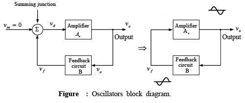 In the block diagram of above figure, vd = vf + vin , vo = Avvd, vf = Bvo
Using these relationships, the following equation is obtained: 
However, vin = 0 and v0 ≠ 0 implies that AvB = 1.
Expressed in polar form, AvB = 1 or total phase shift AvB = 00 or 3600.
Two requirements for oscillations:
(1) The magnitude of the loop gain Av B must be at least 1, and
(2) The total phase shift of the loop gain Av B must be equal to 0o or 360o.
For instance, as indicated in figure, if the amplifier causes a phase shift of 180o, the feedback circuit must provide an additional phase shift of 180o so that the total phase shift around the loop is 360o. The waveforms shown are sinusoidal and are used to illustrate the circuit’s action. The type of waveform generated by an oscillator depends on the components in the circuit and hence may be sinusoidal, square, or triangular. In addition, the frequency of oscillation is determined by the components in the feedback circuit.
- Oscillator Types
Because of their widespread use, many different types of oscillators are available. These oscillator types are summarized in Table given below.
Table: OSCILATOR TYPES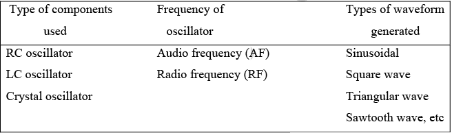
- Frequency Stability
The ability of the oscillator circuit to oscillate at one exact frequency is called frequency stability. Although a number of factors may cause changes in oscillator frequency, the primary factors are temperature changes and the change in dc power supply. Temperature and power supply changes cause variations in the op-amp’s gain, in junction capacitances and resistances of the transistors in an op-amp, and in external circuit components. In most cases these variations can be kept small by careful design, by using regulated power supplies, and by temperature control.
|
91 videos|21 docs|25 tests
|
FAQs on Operational Amplifier - Solid State Physics, Devices & Electronics
| 1. What is an operational amplifier (op-amp)? |  |
| 2. How does an operational amplifier work? | |
| 3. What are the important characteristics of an operational amplifier? | |
| 4. What are some common applications of operational amplifiers? | |
| 5. What are the different types of operational amplifiers? | |


Operational Amplifier | Solid State Physics
,Viva Questions
,video lectures
,MCQs
,Extra Questions
,Summary
,shortcuts and tricks
,Exam
,Operational Amplifier | Solid State Physics
,Semester Notes
,Previous Year Questions with Solutions
,Sample Paper
,Operational Amplifier | Solid State Physics
,ppt
,study material
,past year papers
,Free
,Devices & Electronics
,Important questions
,Devices & Electronics
,Devices & Electronics
,mock tests for examination
,Objective type Questions
,practice quizzes
;


Operational Amplifier Free PDF Download
Importance of Operational Amplifier
Operational Amplifier Notes
Operational Amplifier Physics Questions
Study Operational Amplifier on the App
|
© EduRev
|
Education Revolution
|


|


