Physics Exam  >  Physics Notes  >  Solid State Physics, Devices & Electronics  >  Bipolar Junction Transistors: Assignment

Bipolar Junction Transistors: Assignment | Solid State Physics, Devices & Electronics PDF Download

Q.1. Consider the circuits shown in figures (a) and (b) below
Bipolar Junction Transistors: Assignment | Solid State Physics, Devices & ElectronicsIf the transistors in Figures (a) and (b) have current gain (βdc) of 100 and 10 respectively, then check whether they operate in active region, saturation region or cutoff region. 

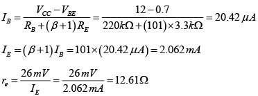
In both case input section is F.B.
For figure (a) Bipolar Junction Transistors: Assignment | Solid State Physics, Devices & Electronics
Thus VCB = VC - VB = (10-2x10)-0.7V = -ve ⇒ Output section is F.B.
Since both sections are F.B. So it is in saturation region.
For figure (b) Bipolar Junction Transistors: Assignment | Solid State Physics, Devices & Electronics
Thus VCB=VC-V= (4-4.3x1)-0.7= -ve
⇒ Since both sections are F.B. So it is in saturation region.


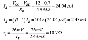
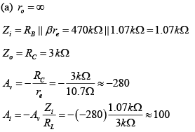
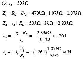
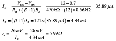
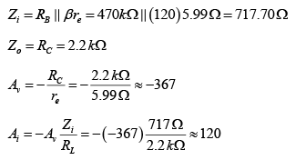
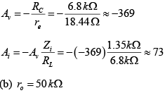
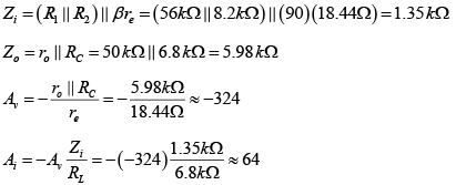
Q.2. For the network shown in figure, determine re, Zi, Zo, Av and Ai. (use re = 26mV/IE)
If (a) ro = ∞
(b) r0 = 50 kΩ
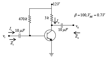
Bipolar Junction Transistors: Assignment | Solid State Physics, Devices & Electronics

DC Analysis:  
Bipolar Junction Transistors: Assignment | Solid State Physics, Devices & Electronics
AC Analysis:  
Bipolar Junction Transistors: Assignment | Solid State Physics, Devices & Electronics


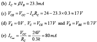
Q.3. Consider the following circuit in which the current gain βdc of the transistor is 100 and VBE = 0.7V.
Find
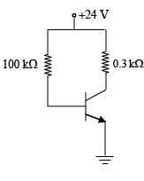
Bipolar Junction Transistors: Assignment | Solid State Physics, Devices & Electronics(a) IB 
(b) IC 
(c) VCE 
(d) VC, VB and VE 
(e) I
C.sat

Bipolar Junction Transistors: Assignment | Solid State Physics, Devices & Electronics


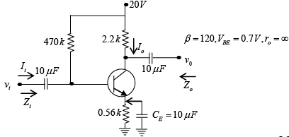
Q.4. For the network shown in figure, determine re, Zi, Zo, Av and Ai. (use re = 26mV/IE)
Bipolar Junction Transistors: Assignment | Solid State Physics, Devices & Electronics

DC Analysis:  
Bipolar Junction Transistors: Assignment | Solid State Physics, Devices & Electronics
AC Analysis:  
RE is “shorted out” by CE for the ac analysis. Therefore
Bipolar Junction Transistors: Assignment | Solid State Physics, Devices & Electronics

Bipolar Junction Transistors: Assignment | Solid State Physics, Devices & Electronics


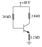
Q.5. Consider the following circuit in which the current gain βdc of the transistor is 100, VBE = 0.7V. Find
Bipolar Junction Transistors: Assignment | Solid State Physics, Devices & Electronics

(a) IB 
(b) IC 
(c) VCE 
(d) VC, VB and VE 
(e) I
C.sat 

Bipolar Junction Transistors: Assignment | Solid State Physics, Devices & Electronics


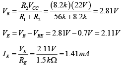
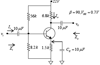
Q.6. For the network shown in figure, determine re, Zi, Zo, Av and Ai. (use re = 26mV/IE)
If (a) ro = ∞
(b) ro = 50kΩ
Bipolar Junction Transistors: Assignment | Solid State Physics, Devices & Electronics

DC Analysis:  
βRE = 90 x 1.5 = 135kΩ and 10R2 = 10 x 8.2 = 82kΩ
Thus βRE >> 10R2 (Use approximate meathod)
Bipolar Junction Transistors: Assignment | Solid State Physics, Devices & Electronics
AC Analysis:  
(a) ro = ∞
Bipolar Junction Transistors: Assignment | Solid State Physics, Devices & Electronics


Q.7. For the transistor circuit shown below, evaluate VE, RB and RC, given IC = 1mA, β = 80, VCE = 3.8 V, VBE = 0.7 V and VCC = 10V use the approximation IC ≈ IE.
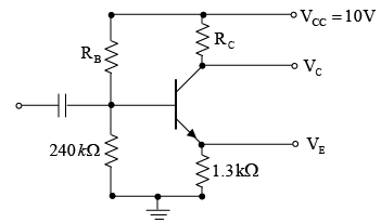
Bipolar Junction Transistors: Assignment | Solid State Physics, Devices & Electronics

Bipolar Junction Transistors: Assignment | Solid State Physics, Devices & Electronics

Bipolar Junction Transistors: Assignment | Solid State Physics, Devices & Electronics
Applying KVL to input section,
Bipolar Junction Transistors: Assignment | Solid State Physics, Devices & Electronics
Writing Kirchhoff’s voltage law for the indicated loop in the clockwise direction will result in - IERE - VCE - ICRC + VCC = 0
Bipolar Junction Transistors: Assignment | Solid State Physics, Devices & Electronics

Bipolar Junction Transistors: Assignment | Solid State Physics, Devices & Electronics


Q.8. For the network shown in figure, determine re, Zi, Zo, Av and Ai. (use re = 26mV/IE)
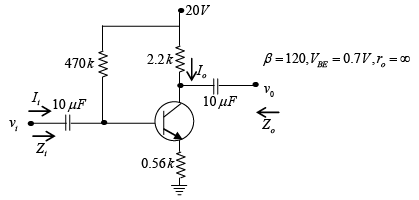
Bipolar Junction Transistors: Assignment | Solid State Physics, Devices & Electronics

DC Analysis:  
Bipolar Junction Transistors: Assignment | Solid State Physics, Devices & Electronics
AC Analysis:  
Bipolar Junction Transistors: Assignment | Solid State Physics, Devices & Electronics


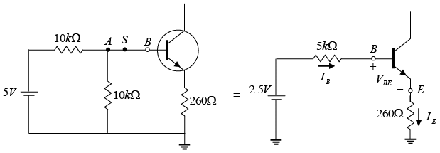
Q.9. For the transistor shown in the figure, the dc current gain βdc = 50 and VBE = 0.7. The switch S is initially open. 
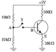
Bipolar Junction Transistors: Assignment | Solid State Physics, Devices & Electronics

(a) Calculate the voltage at point A. If the switch S is now closed, what would be the voltage at point A?      
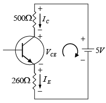
(b) Draw the dc load line and find the Q-point of the circuit with the switch S remaining closed.  

(a) When switch S is open Bipolar Junction Transistors: Assignment | Solid State Physics, Devices & Electronics 

Bipolar Junction Transistors: Assignment | Solid State Physics, Devices & ElectronicsWhen switch S is closed, draw Thevenin’s equivalent circuit
Bipolar Junction Transistors: Assignment | Solid State Physics, Devices & Electronics

Bipolar Junction Transistors: Assignment | Solid State Physics, Devices & Electronics
Applying KVL to input section,
Bipolar Junction Transistors: Assignment | Solid State Physics, Devices & Electronics
(b) Writing Kirchhoff’s voltage law for the indicated loop in the clockwise direction will result in - IERE - VCE - ICRC + VCC = 0
Bipolar Junction Transistors: Assignment | Solid State Physics, Devices & Electronics

Bipolar Junction Transistors: Assignment | Solid State Physics, Devices & Electronics
Thus Q -point is (IC, VCE) (5.0 mA,1.2 V).


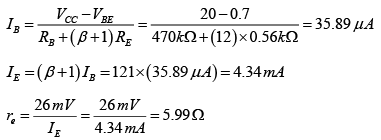
Q.10. For the network shown in figure, determine re, Zi, Zo, Av and Ai. (use re = 26mV/IE)
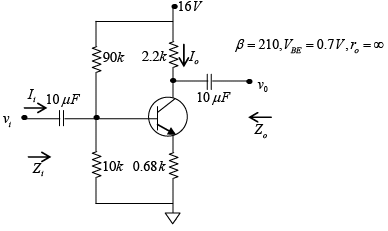
Bipolar Junction Transistors: Assignment | Solid State Physics, Devices & Electronics

DC Analysis:  
Bipolar Junction Transistors: Assignment | Solid State Physics, Devices & Electronics
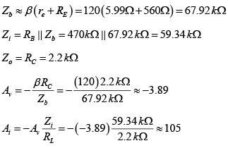
AC Analysis:  
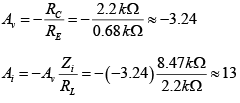
Zi = (R1||R2) || Zb = (R1 || R2) || βRE = (90kΩ||10kΩ) || (210) (0.68kΩ) = 8.47 kΩ
Zo = RC = 2.2 kΩ
Bipolar Junction Transistors: Assignment | Solid State Physics, Devices & Electronics


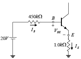
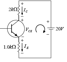
Q.11. For the transistor circuit shown in the figure βdc = 100 and 0.7 VBE = V. Determine the base current IB, the collector-emitter voltage VCE, the emitter voltage VE, the base voltage VB and the saturation current ICsat.
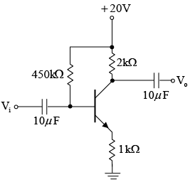
Bipolar Junction Transistors: Assignment | Solid State Physics, Devices & Electronics

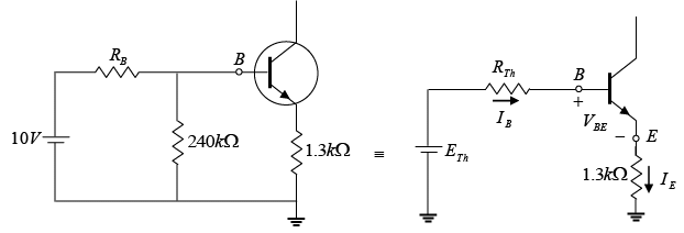
Drawing Equivalent circuit for input section
Applying KVL to input section, -20 + 450 x IB + 0.7 + 1.0 x IE = 0
⇒ -20 + 450 x IB + 0.7 + 1.0 x βIB = 0
∵ IE ≈ βIB
Bipolar Junction Transistors: Assignment | Solid State Physics, Devices & Electronics

Bipolar Junction Transistors: Assignment | Solid State Physics, Devices & Electronics

Bipolar Junction Transistors: Assignment | Solid State Physics, Devices & Electronics
⇒ VB = VBE + IERE = 0.7 + 3.5 = 4.2V
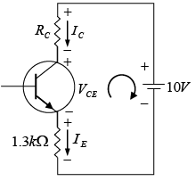
Writing Kirchhoff’s voltage law for the indicated loop in the clockwise direction will result in - IERE - VCE - ICRC + VCC = 0

Bipolar Junction Transistors: Assignment | Solid State Physics, Devices & ElectronicsBipolar Junction Transistors: Assignment | Solid State Physics, Devices & Electronics


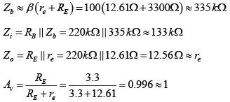
Q.12. For the network shown in figure, determine re, Zi, Zo, and Av. (use re = 26mV/IE)
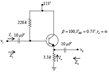
Bipolar Junction Transistors: Assignment | Solid State Physics, Devices & Electronics

It’s a common collector configuration.
DC Analysis:  
Bipolar Junction Transistors: Assignment | Solid State Physics, Devices & Electronics
AC Analysis:  
Bipolar Junction Transistors: Assignment | Solid State Physics, Devices & Electronics 


Q.13. Determine the dc level of IB and VC for the network shown in figure below.
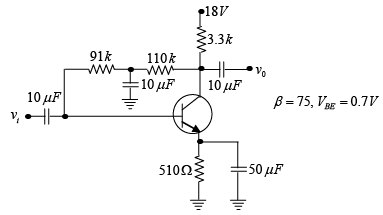
Bipolar Junction Transistors: Assignment | Solid State Physics, Devices & Electronics

In DC equivalent, capacitor is open circuited.
Bipolar Junction Transistors: Assignment | Solid State Physics, Devices & Electronics


Q.14. Determine the dc level of VC and VB for the network shown in figure below.
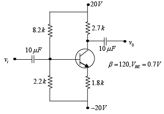
Bipolar Junction Transistors: Assignment | Solid State Physics, Devices & Electronics

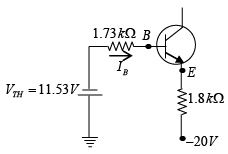
In DC equivalent, capacitor is open circuited. Let’s draw Thevenin’s equivalent circuit for input section.
Bipolar Junction Transistors: Assignment | Solid State Physics, Devices & ElectronicsBipolar Junction Transistors: Assignment | Solid State Physics, Devices & Electronics and RTH = 8.2k||2.2k = 1.73k
11.53 + IB x 1.73 + 0.7 + βIB x 1.8 - 20 = 0
⇒ IB = 35.39μA
Bipolar Junction Transistors: Assignment | Solid State Physics, Devices & Electronics
VB = -VTH - IBRTH = -11.53 - 35.39μA x 1.73k = -11.59V
Bipolar Junction Transistors: Assignment | Solid State Physics, Devices & Electronics


Q.15. Determine the dc level of VCE and IE for the network shown in figure below.
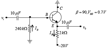
Bipolar Junction Transistors: Assignment | Solid State Physics, Devices & Electronics

Applying KVL to input section
IB x 240 + 0.7 + 90 x IB x 2 - 20 = 0 ⇒ IB = 45.73μA
Bipolar Junction Transistors: Assignment | Solid State Physics, Devices & Electronics
Applying KVL to output section
Bipolar Junction Transistors: Assignment | Solid State Physics, Devices & Electronics


Q.16. Given that Bipolar Junction Transistors: Assignment | Solid State Physics, Devices & Electronicsdetermine  R1 and RC for the network shown in figure below.
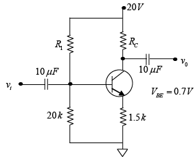
Bipolar Junction Transistors: Assignment | Solid State Physics, Devices & Electronics
Bipolar Junction Transistors: Assignment | Solid State Physics, Devices & Electronics
Bipolar Junction Transistors: Assignment | Solid State Physics, Devices & Electronics 

The document Bipolar Junction Transistors: Assignment | Solid State Physics, Devices & Electronics is a part of the Physics Course Solid State Physics, Devices & Electronics.
All you need of Physics at this link: Physics
91 videos|21 docs|25 tests

FAQs on Bipolar Junction Transistors: Assignment - Solid State Physics, Devices & Electronics

1. What is a bipolar junction transistor?
Ans. A bipolar junction transistor (BJT) is a three-layer semiconductor device that can amplify or switch electronic signals and electrical power. It consists of two pn junctions, namely the emitter-base junction (forward-biased) and the base-collector junction (reverse-biased).
2. What are the different types of bipolar junction transistors?
Ans. There are two main types of bipolar junction transistors: NPN (Negative-Positive-Negative) and PNP (Positive-Negative-Positive). In an NPN transistor, the majority charge carriers are electrons, while in a PNP transistor, the majority charge carriers are holes.
3. How does a bipolar junction transistor work?
Ans. A BJT operates by controlling the flow of charge carriers (electrons or holes) between its three layers - emitter, base, and collector. By applying a small current or voltage at the base-emitter junction, a much larger current can flow from the collector to the emitter, allowing amplification or switching of signals.
4. What are the applications of bipolar junction transistors?
Ans. Bipolar junction transistors have a wide range of applications in electronic devices and circuits. They are commonly used in amplifiers, oscillators, switches, voltage regulators, and digital logic circuits. They are also used in radio and television receivers, audio systems, and power supply circuits.
5. What are the advantages and disadvantages of bipolar junction transistors?
Ans. The advantages of bipolar junction transistors include high current gain, high frequency response, and low noise. They also have good linearity and temperature stability. However, they have some disadvantages such as higher power consumption, larger size compared to other transistors, and lower power handling capability compared to some other devices like MOSFETs.
91 videos|21 docs|25 tests
Download as PDF
Explore Courses for Physics exam
Signup for Free!
Signup to see your scores go up within 7 days! Learn & Practice with 1000+ FREE Notes, Videos & Tests.
10M+ students study on EduRev
Related Searches

Bipolar Junction Transistors: Assignment | Solid State Physics

,

practice quizzes

,

Devices & Electronics

,

video lectures

,

Bipolar Junction Transistors: Assignment | Solid State Physics

,

Free

,

ppt

,

Devices & Electronics

,

study material

,

shortcuts and tricks

,

mock tests for examination

,

pdf

,

Summary

,

Devices & Electronics

,

past year papers

,

Bipolar Junction Transistors: Assignment | Solid State Physics

,

Extra Questions

,

MCQs

,

Viva Questions

,

Semester Notes

,

Sample Paper

,

Important questions

,

Objective type Questions

,

Exam

,

Previous Year Questions with Solutions

;