Current Components in Semiconductor | Solid State Physics, Devices & Electronics PDF Download
➤ Drift Current (Conductivity and Mobility)
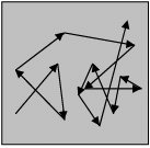
The charge carriers in a solid are in constant motion, even at thermal equilibrium. At room temperature, for example, the thermal motion of an individual electron may be visualized as random scattering from lattice atoms, impurities, other electrons, and defects. Since the scattering is random, there is no net motion of the group of n electrons/ cm3 over any period of time. This is not true of an individual electron, of course. The probability of the electron in returning to its starting point after some time t is negligibly small. However, if a large number of electrons is considered (e.g. 1016 cm−3 in an n-type semiconductor), there will be no preferred direction of motion for the group of electrons and no net current flow.

Figure : Thermal motion of an electron in a solid.
If an electric field Ex is applied in the x-direction, each electron experiences a net force −qEx from the field. This force may be insufficient to alter appreciably the random path of an individual electron; the effect when averaged over all the electrons, however, is a net motion of the group in the x-direction. If px is the x-component of the total momentum of the group, force of the field on the n electrons / cm3 is Initially, above equation seems to indicate a continuous acceleration of the electrons in the − x -direction. This is not the case, however, because the net acceleration is just balanced in steady state by the decelerations of the collision processes. Thus while the steady field Ex does produce a net momentum p− x , the net rate of change of momentum when collisions are included must be zero in the case of steady state current flow.
To find the total rate of momentum change from collisions, we must investigate the collision probabilities more closely. If the collisions are truly random, there will be a constant probability of collision at any time for each electron. Let us consider a group of
N0 electrons at time t = 0 and define N (t) as the number of electrons that have not undergone a collision by time t. The rate of decrease in N (t) at any time t is proportional to the number left unscattered at t,  where t−1 is a constant proportionality.
The solution to above equation is an exponential function N(t) = N0e−t/ and
and  represents the mean time between scattering events, called the mean free time. The probability that any electron has a collision in the time interval dt is dt/
 .Thus the differential change in p, due to collisions in time dt is
  The rate of change of px , due to the decelerating effect of collisions is
  The sum of acceleration and deceleration effects must be zero for steady state. Thus
  The average momentum per electron is
  where the angular brackets indicate an average over the entire group of electrons. As expected for steady state, the above equation indicates that the electrons have on the average a constant net velocity in the negative x-direction:
 Actually, the individual electrons move in many directions by thermal motion during a given time period, but (vx) tells us the net drift of an average electron in response to the electric field. The drift speed (vx) is usually much smaller than the random speed due to thermal motion vth.
The current density resulting from this net drift is just the number of electrons crossing a unit area per unit time (n(vx)) multiplied by the charge on the electron ( −q ) : Thus the current density is proportional to the electric field, as we expect from Ohm's law:
 The conductivity σ ( Ω− cm)−1 can be written
  The quantity μn, called the electron mobility, describes the ease with which electrons drift in the material. Mobility is a very important quantity in characterizing semiconductor materials and in device development.
The mobility can be expressed as the average particle drift velocity per unit electric field. Thus  and units of mobility are (cm/s) /(V/cm) = cm2 / V - s . The minus sign in the definition results in a positive value of mobility, since electrons drift opposite to the field.
The current density can be written in terms of mobility as Jx =qnμnEx.
This derivation has been based on the assumption that the current is carried primarily by electrons. For hole conduction we change n to p , −q to + q , μn to μp
where  is the mobility for holes. If both electrons and holes participate, then where
For N-type semiconductor
 where nn and pn are electron and hole concentration in N-type.
For P-type semiconductor since PP >>nP where np and pp are electron and hole concentration in P-type.
Example: The following data are given for intrinsic Germanium at 300 K . ni = 2.4×10¹⁹ /m3 , μe = 0.39m2V−1s−1, μp = 0.19m2V−1s−1. Find the conductivity of the Germanium.
Solution: 
Example: A sample of Si has electron and hole mobilities of 0.13 and 0.05 m2V −1s −1 respectively at 300K. It is doped with P and Al with doping densities of 1.5 × 10²¹ / m3 and 2.5 × 10²¹ / m3 respectively. The resistivity of doped Si sample at 300K is
(a) 0.125 Ωm
(b) 8.0 Ωm
(c) 2.125 Ωm
(d) 0.225 Ωm
Solution: Resulting doped crystal is p-type and pP = (2.5-1.5)x1021/m3 = 1 x 10²¹/m3
➤ Diffusion Current
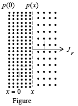
In addition to a conduction current, the transport of charges in a semiconductor may be accounted for a mechanism called diffusion. It is possible to have non-uniform concentration of particles in a semiconductor. As indicated in the figure, the concentration p of holes varies with distance x in the semiconductor, and there exist a concentration gradient, dp/dx in the density of the carriers.

The existence of a gradient implies that if an imaginary surface is drawn in the semiconductor, the density of the holes immediately on one side of the surface is larger than the density on the other side. The holes are in random motion as a result of their thermal energy. Accordingly, holes will continue to move back and forth across this surface. We may then expect that, in a given time interval, more holes will cross the surface
Note: It should be noted that this net transport of charge is not the result of mutual repulsion among charges of like sign, but is simply the result of a statistical phenomenon. This diffusion is exactly analogous to that which occurs in a neutral gas if concentration gradient exists in the gaseous container.
The diffusion hole-current density Jp (ampere per square meter) is proportional to the concentration gradient, and is given by:  where Dp (Square meters/second) is called diffusion constant. Since p decreases with increasing x , then dp/dx = is negative and the minus sign needed, so that J p is positive in the positive x -direction.
Similarly, 
➤ Einstein Relationship
Since both diffusion and mobility are statistical thermodynamic phenomena, D and μ are not independent. The relationship between them is given by  where VT is the ‘Volt-equivalent of temperature’.
  k → Boltzmann constant in electron volts per degree KelvinAt room temperature T = 3000K , VT =0.026 V ⇒ μ= 39D
➤ Total Current in a Semiconductor
It is possible for both a potential gradient and a concentration gradient to exist simultaneously within a semiconductor. In such a situation, the total hole current is the sum of the drift current and the diffusion current,  Similarly the net electron current is:
Effects of Temperature and Doping on Mobility
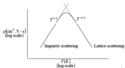
The two basic types of scattering mechanisms that influence electron and hole mobility are lattice scattering and impurity scattering. In lattice scattering a carrier moving through the crystal is scattered by a vibration of the lattice, resulting from the temperature (Collective vibrations of atoms in the crystal are called phonons. Thus lattice scattering is also known as phonon scattering). The frequency of such scattering events increases as the temperature increases, since the thermal agitation of the lattice becomes greater. Therefore, we should expect the mobility to decrease as the sample is heated. On the other hand, scattering from crystal defects such as ionized impurities becomes the dominant mechanism at low temperatures. Since the atoms of the cooler lattice are less agitated, lattice scattering is less important; however, the thermal motion of the carriers is also slower.
 Figure : Approximate temperature dependence of mobility with both lattice and impurity scattering.
Since a slowly moving carrier is likely to be scattered more strongly by an interaction with a charged ion than is a carrier with greater momentum, impurity scattering events cause a decrease in mobility with decreasing temperature. The approximate temperature dependencies are T−3/2 for lattice scattering and T3/2 for impurity scattering.
The Potential Variation within a Graded Semiconductor
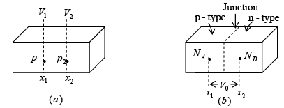
 Figure (a): A graded semiconductor: p(x) is not constant
(b): One portion is doped with (uniformly) acceptor ions and the other section is doped uniformly with donor ions so that a metallurgical junction is formed.
Consider a semiconductor where the hole concentration p is a function of x; that is, the doping is non-uniform or graded. Assume a steady-state situation and zero excitation; that is, no carriers are injected into the specimen from any external source. With no excitation there can be no steady movement of charge in the bar, although the carriers possess random motion due to thermal agitation. Hence the total hole current must be zero (also, the total electron current must be zero). Since p is not constant, we expect a non-zero hole diffusion current. In order for the total hole current to vanish there must exist a hole drift current which is equal and opposite to the diffusion current. However, conduction current requires an electric field and hence we conclude that, as a result of the non-uniform doping, an electric field is generated within the semiconductor. We shall now find this field and the corresponding potential variation throughout the bar.
Since  If the doping concentration p(x) is known, this equation allows the built in field E (x) to be calculated.
 If this equation is integrated between x1 , where the concentration is p1 and the potential is V1 and x2 where p = p2 and V =V2 , the result is:
  Note: The potential difference between two points depends only upon the concentration at these points and is independent of their separation (x2 − x1).
Above equation can be put in the form p1 = p2 eV21/VT
This is the Boltzmann relationship of kinetic gas theory.
Starting with Jn = 0 and proceeding as above, the Boltzmann equation for electrons is obtained as n1 = n2e-V21/VT. Now n1p1 = n2p2.
This equation states that the product np is a constant independent of x , and hence the amount of doping, under thermal equilibrium.
For an intrinsic semiconductor n = p = ni and hence np = ni2.
➤ An Open-Circuited Step-graded Junction
Consider the special case indicated in figure (b). The left half of the bar is p-type with a constant concentration NA , whereas the right-half is n-type with a uniform density ND. The dashed plane is a metallurgical ( p − n ) junction separating the two sections with different concentrations. This type of doping where the density changes abruptly from p to n type is called step-grading. The step graded junction is located at the plane where the concentration is zero. The above theory indicates that there is built-in potential between these two sections (called the contact difference of potential Vo.)
Thus  Because p1 = ppo thermal-equilibrium hole concentration in p-side
p2=pne thermal equilibrium hole concentration in n-side
since 
➤ Summary
1. In a semiconductor two types of mobile charge carriers are available. The bipolar nature of a semiconductor is to be contrasted with the unipolar property of a metal, which possesses only free electrons.
2. A semiconductor may be fabricated with donor (acceptor) impurities. So it contains mobile charges which are primarily electrons (holes).
3. The intrinsic carrier concentration is a function of temperature. At room temperature, essentially all donors or acceptors are ionized.
4. Current is due to two distinct phenomenons:
(a) Carriers drift in an electric field (this conduction current is also available in metals).
(b) Carriers diffuse if a concentration gradient exists (a phenomenon, which does not take place in metals).
5. Carriers are continuously being generated (due to thermal creation of hole-electron pairs) and are simultaneously disappearing (due to recombination).
6. The fundamental law governing the flow of charges is called the continuity equation. It is formulated by considering that charges can neither be created nor destroyed if generation, recombination, drift and diffusion are all taken into account.
7. If the minority carriers are injected into a region containing majority carriers, then usually the injected minority concentration is very small compared with the density of the majority carries. For this low-level injection condition the minority current is predominantly due to diffusion; in other words, the minority drift current may be neglected.
8. The total majority-carrier flow is the sum of a drift and diffusion current. The majority conduction current results from a small electric field internally created within the semiconductor because of the injected carriers.
9. The minority-carrier concentration injected into one end of a semiconductor bar decreases exponentially with distance into the specimen (as a result of diffusion and recombination).
10. Across an open-circuited p-n junction there exists a contact difference of potential.
|
91 videos|21 docs|25 tests
|
FAQs on Current Components in Semiconductor - Solid State Physics, Devices & Electronics
| 1. What are the current components in a semiconductor? |  |
| 2. What is the role of electrons in a semiconductor? |  |
| 3. How do holes contribute to current flow in a semiconductor? |  |
| 4. What is the significance of current components in semiconductor devices? |  |
| 5. How do current components affect the performance of semiconductor devices? |  |


