SR flip flop | Digital Circuits - Electronics and Communication Engineering (ECE) PDF Download
| Table of contents |
|
| Introduction |
|
| Typical applications for SR Flip-flops. |
|
| The SR Flip-flop. |
|
| Problems with the SR Flip-flop |
|

Introduction
- The SR flip flop is a 1-bit memory bistable device having two inputs, i.e., SET and RESET. The SET input 'S' set the device or produce the output 1, and the RESET input 'R' reset the device or produce the output 0. The SET and RESET inputs are labeled as S and R, respectively.
- The SR flip flop stands for "Set-Reset" flip flop. The reset input is used to get back the flip flop to its original state from the current state with an output 'Q'. This output depends on the set and reset conditions, which is either at the logic level "0" or "1".
- The NAND gate SR flip flop is a basic flip flop which provides feedback from both of its outputs back to its opposing input. This circuit is used to store the single data bit in the memory circuit. So, the SR flip flop has a total of three inputs, i.e., 'S' and 'R', and current output 'Q'. This output 'Q' is related to the current history or state. The term "flip-flop" relates to the actual operation of the device, as it can be "flipped" to a logic set state or "flopped" back to the opposing logic reset state.
The NAND Gate SR Flip-Flop
We can implement the set-reset flip flop by connecting two cross-coupled 2-input NAND gates together. In the SR flip flop circuit, from each output to one of the other NAND gate inputs, feedback is connected. So, the device has two inputs, i.e., Set 'S' and Reset 'R' with two outputs Q and Q' respectively. Below are the block diagram and circuit diagram of the S-R flip flop.
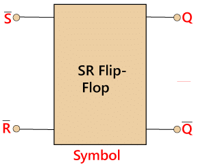
Block Diagram:
Circuit Diagram:
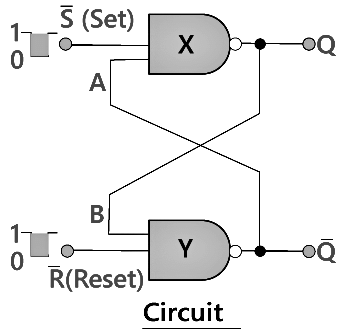
The Set State
In the above diagram, when the input R is set to false or 0 and the input S is set to true or 1, the NAND gate Y has an input 0, which will produce the output Q' 1. The value of Q' is faded to the NAND gate 'X' as input 'A', and now both the inputs of the NAND gate 'X' are 1(S=A=1), which will produce the output 'Q' 0.
Now, if the input R is changed to 1 with 'S' remaining 1, the inputs of NAND gate 'Y' is R=1 and B=0. Here, one of the inputs is also 0, so the output of Q' is 1. So, the flip flop circuit is set or latched with Q=0 and Q'=1.
Reset State
The output Q' is 0, and output Q is 1 in the second stable state. It is given by R =1 and S = 0. One of the inputs of NAND gate 'X' is 0, and its output Q is 1. Output Q is faded to NAND gate Y as input B. So, both the inputs to NAND gate Y are set to 1, therefore, Q' = 0.
f the input S is changed to 0 with 'R' remaining 1, the output Q' will be 0 and there is no change in state. So, the reset state of the flip flop circuit has been latched, and the set/reset actions are defined in the following truth table:
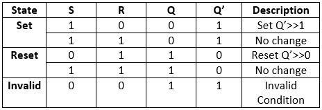
From the above truth table, we can see that when set 'S' and reset 'R' inputs are set to 1, the outputs Q and Q' will be either 1 or 0. These outputs depend on the input state S or R before the input condition exist. So, when the inputs are 1, the states of the outputs remain unchanged.
The condition in which both the inputs states are set to 0 is treated as invalid and must be avoided.
Typical applications for SR Flip-flops.
The basic building bock that makes computer memories possible, and is also used in many sequential logic circuits is the flip-flop or bi-stable circuit. Just two inter-connected logic gates make up the basic form of this circuit whose output has two stable output states. When the circuit is triggered into either one of these states by a suitable input pulse, it will ‘remember’ that state until it is changed by a further input pulse, or until power is removed. For this reason the circuit may also be called a Bi-stable Latch.
The SR flip-flop can be considered as a 1-bit memory, since it stores the input pulse even after it has passed. Flip-flops (or bi-stables) of different types can be made from logic gates and, as with other combinations of logic gates, the NAND and NOR gates are the most versatile, the NAND being most widely used. This is because, as well as being universal, i.e. it can be made to mimic any of the other standard logic functions, it is also cheaper to construct. Other, more widely used types of flip-flop are the JK, the D type and T type, which are developments of the SR flip-flop and will be studied in Modules 5.3 and 5.4.
The SR Flip-flop.
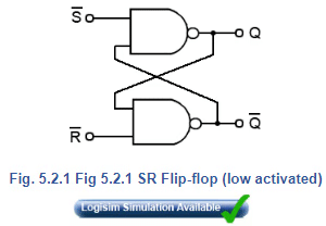
The SR (Set-Reset) flip-flop is one of the simplest sequential circuits and consists of two gates connected as shown in Fig. 5.2.1. Notice that the output of each gate is connected to one of the inputs of the other gate, giving a form of positive feedback or ‘cross-coupling’.
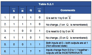
The circuit has two active low inputs marked S and R, ‘NOT’ being indicated by the bar above the letter, as well as two outputs, Q and Q. Table 5.2.1 shows what happens to the Q and Q outputs when a logic 0 is applied to either the S or R inputs.
The SR Flip-flop Truth Table (Table 5.2.1)
- Q output is set to logic 1 by applying logic 0 to the
 input.
 - Returning the S input to logic 1 has no effect. The 0 pulse (high-low-high) has been ‘remembered’ by the Q.
- Q is reset to 0 by logic 0 applied to the
 input.
 - As returns to logic 1 the 0 on Q is ‘remembered’ by Q.
Problems with the SR Flip-flop
There are however, some problems with the operation of this most basic of flip-flop circuits. For conditions 1 to 4 in Table 5.2.1,  is the inverse of Q. However, in row 5 both inputs are 0, which makes both Q and = 1, and as they are no longer opposite logic states, although this state is possible, in practical circuits it is ‘not allowed’.
In row 6 both inputs are at logic 1 and the outputs are shown as ‘indeterminate’, this means that although Q and will be at opposite logic states it is not certain whether Q will be 1 or 0, Notice however that in the absence of any input pulses, both inputs are normally at logic 1. This is normally OK, as the outputs will be at the state remembered from the last input pulse. The indeterminate or uncertain logic state only occurs if the inputs change from 0,0 to 1,1 together. This should be avoided in normal operation, but is likely to happen when power is first applied. This could lead to uncertain results, but the flip-flop will work normally once an input pulse is applied to either input.
The SR Flip-flop is therefore, a simple 1-bit memory. If the S input is taken to logic 0 then back to logic 1, any further logic 0 pulses at will have no effect on the output.
|
76 videos|175 docs|70 tests
|
FAQs on SR flip flop - Digital Circuits - Electronics and Communication Engineering (ECE)
| 1. What is an SR Flip-flop and how does it function? |  |
| 2. What are typical applications of SR Flip-flops? | |
| 3. What are the problems associated with SR Flip-flops? | |
| 4. How can the issues with SR Flip-flops be resolved? | |
| 5. Can SR Flip-flops be used in synchronous circuits? | |


Sample Paper
,shortcuts and tricks
,Viva Questions
,Extra Questions
,video lectures
,study material
,past year papers
,Previous Year Questions with Solutions
,mock tests for examination
,Free
,MCQs
,Important questions
,Objective type Questions
,ppt
,SR flip flop | Digital Circuits - Electronics and Communication Engineering (ECE)
,SR flip flop | Digital Circuits - Electronics and Communication Engineering (ECE)
,practice quizzes
,Exam
,Summary
,SR flip flop | Digital Circuits - Electronics and Communication Engineering (ECE)
,Semester Notes
;


SR flip flop Free PDF Download
Importance of SR flip flop
SR flip flop Notes
SR flip flop Electronics and Communication Engineering (ECE) Questions
Study SR flip flop on the App
|
© EduRev
|
Education Revolution
|


|


