Half Adder & Full Adder | Digital Circuits - Electronics and Communication Engineering (ECE) PDF Download
| Table of contents |
|
| Half Adder |
|
| Full Adder |
|
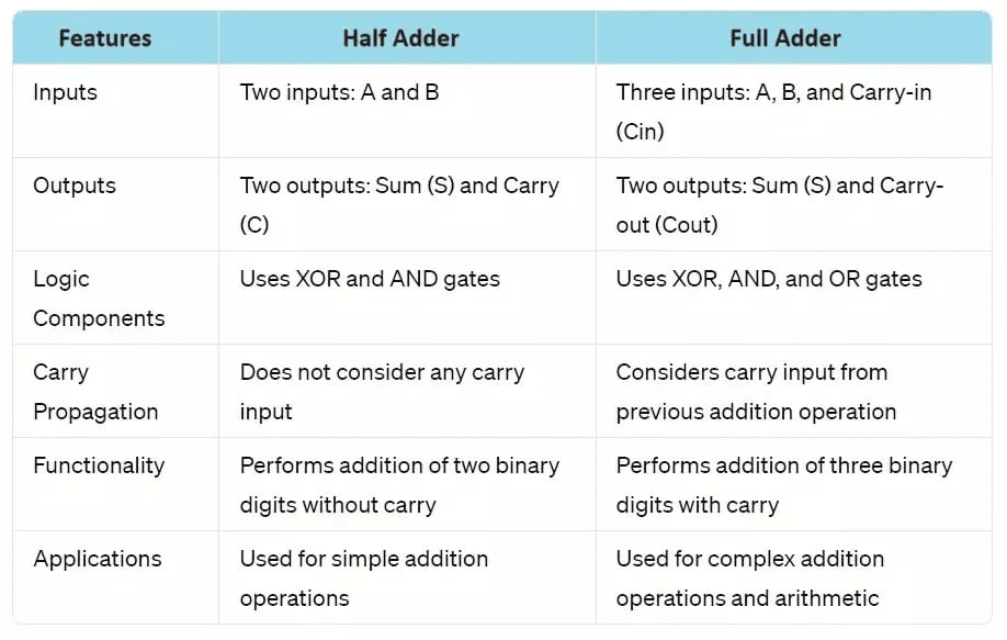
| Differentiate Between Half Adder and Full Adder |
|
| Conclusion |
|
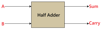
Half Adder
The Half-Adder is a basic building block of adding two numbers as two inputs and produce out two outputs. The adder is used to perform OR operation of two single bit binary numbers. The augent and addent bits are two input states, and 'carry' and 'sum 'are two output states of the half adder.Block diagram

Truth Table
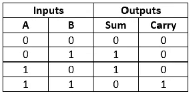
In the above table,
- 'A' and' B' are the input states, and 'sum' and 'carry' are the output states.
- The carry output is 0 in case where both the inputs are not 1.
- The least significant bit of the sum is defined by the 'sum' bit.
The SOP form of the sum and carry are as follows:
Sum = x'y + xy
Carry = xy
Construction of Half Adder Circuit
In the block diagram, we have seen that it contains two inputs and two outputs. The augent and addent bits are the input states, and carry and sum are the output states of the half adder. The half adder is designed with the help of the following two logic gates:- 2-input AND Gate.
- 2-input Exclusive-OR Gate or Ex-OR Gate
1. 2-input Exclusive-OR Gate or Ex-OR Gate
The Sum bit is generated with the help of the Exclusive-OR or Ex-OR Gate.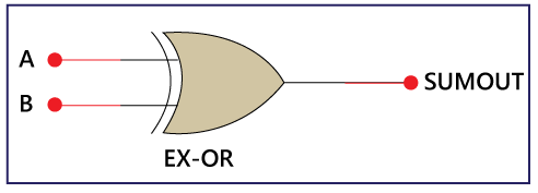 The above is the symbol of the EX-OR gate. In the above diagram, 'A' and 'B' are the inputs, and the 'SUMOUT' is the final outcome after performing the XOR operation of both numbers.
The truth table of the EX-OR gate is as follows: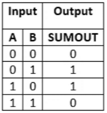 From the above table, it is clear that the XOR gate gives the result 1 when both of the inputs are different. When both of the inputs are the same, the XOR gives the result 0. To learn more about the XOR gate.
2. 2-input AND Gate
The XOR gate is unable to generate the carry bit. For this purpose, we use another gate called AND Gate. The AND gate gives the correct result of the carry.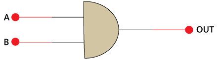
The above is the symbol of the AND gate. In the above diagram, 'A' and 'B' are the inputs, and 'OUT' is the final outcome after performing AND operation of both numbers.
There is the following truth table of AND Gate: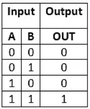 From the above table, it is clear that the AND gate gives the result 1 when both of the inputs are 1. When both of the inputs are different and 0, the AND gates gives the result 0. To learn more about the AND gate.
 |
Test: Adders
|
Start Test |
Half-Adder logical circuit
So, the Half Adder is designed by combining the 'XOR' and 'AND' gates and provide the sum and carry.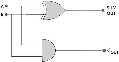 Half-Adder CircuitThere is the following Boolean expression of Half Adder circuit:
Sum= A XOR B (A + B)
Carry= A AND B (A . B)
Full Adder
The half adder is used to add only two numbers. To overcome this problem, the full adder was developed. The full adder is used to add three 1-bit binary numbers A, B, and carry C. The full adder has three input states and two output states i.e., sum and carry.
Block diagram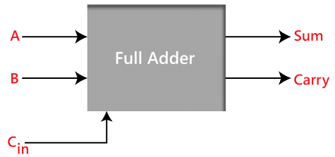
Truth Table
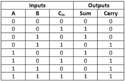 In the above table,
- 'A' and' B' are the input variables. These variables represent the two significant bits which are going to be added
- 'Cin' is the third input which represents the carry. From the previous lower significant position, the carry bit is fetched.
- The 'Sum' and 'Carry' are the output variables that define the output values.
- The eight rows under the input variable designate all possible combinations of 0 and 1 that can occur in these variables.
Note: We can simplify each of the output 'Boolean function' with the help of the unique map method.
The SOP form can be obtained with the help of K-map as: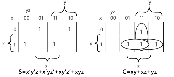 Sum = x' y' z + x' yz + xy' z' + xyz
Carry = xy + xz + yz
Construction of Half Adder Circuit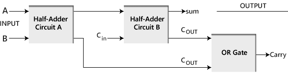
The above block diagram describes the construction of the Full adder circuit. In the above circuit, there are two half adder circuits that are combined using the OR gate. The first half adder has two single-bit binary inputs A and B. As we know that, the half adder produces two outputs, i.e., Sum and Carry. The 'Sum' output of the first adder will be the first input of the second half adder, and the 'Carry' output of the first adder will be the second input of the second half adder. The second half adder will again provide 'Sum' and 'Carry'. The final outcome of the Full adder circuit is the 'Sum' bit. In order to find the final output of the 'Carry', we provide the 'Carry' output of the first and the second adder into the OR gate. The outcome of the OR gate will be the final carry out of the full adder circuit.
The MSB is represented by the final 'Carry' bit.
The full adder logic circuit can be constructed using the 'AND' and the 'XOR' gate with an OR gate.
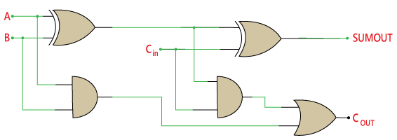 Full-Adder CircuitThe actual logic circuit of the full adder is shown in the above diagram. The full adder circuit construction can also be represented in a Boolean expression.
Sum
- Perform the XOR operation of input A and B.
- Perform the XOR operation of the outcome with carry. So, the sum is (A XOR B) XOR Cin which is also represented as:
- (A ⊕ B) ⊕ Cin
 |
Download the notes
Half Adder & Full Adder
|
Download as PDF |
Carry
- Perform the 'AND' operation of input A and B.
- Perform the 'XOR' operation of input A and B.
- Perform the 'OR' operations of both the outputs that come from the previous two steps. So the 'Carry' can be represented as:
- A.B + (A ⊕ B)
Differentiate Between Half Adder and Full Adder
Conclusion
The half adder and full adder are fundamental components in digital electronics, serving as the building blocks for binary addition. While the half adder efficiently handles the addition of two single-bit binary numbers, producing a sum and carry output using an XOR and AND gate combination, the full adder extends this capability by incorporating a third input for the carry-in, making it suitable for multi-bit addition. By combining two half adders with an OR gate, the full adder effectively computes the sum and carry for three input bits, demonstrating a scalable and robust design for arithmetic operations in digital circuits. This progression from half adder to full adder exemplifies how simple logic gates can be orchestrated to perform complex computational tasks, forming the foundation of modern computing systems.
|
8 videos|84 docs|52 tests
|
FAQs on Half Adder & Full Adder - Digital Circuits - Electronics and Communication Engineering (ECE)
| 1. What is a Half Adder and how does it work? |  |
| 2. What are the main components of a Half Adder? | |
| 3. How is a Half Adder different from a Full Adder? | |
| 4. Can you provide the truth table for a Half Adder? | |
| 5. What are practical applications of Half Adders in digital circuits? | |


Previous Year Questions with Solutions
,Sample Paper
,Half Adder & Full Adder | Digital Circuits - Electronics and Communication Engineering (ECE)
,video lectures
,MCQs
,practice quizzes
,Exam
,Half Adder & Full Adder | Digital Circuits - Electronics and Communication Engineering (ECE)
,shortcuts and tricks
,Objective type Questions
,Half Adder & Full Adder | Digital Circuits - Electronics and Communication Engineering (ECE)
,Important questions
,Semester Notes
,Viva Questions
,Extra Questions
,mock tests for examination
,Summary
,past year papers
,Free
,ppt
,study material
,


Half Adder & Full Adder Free PDF Download
Importance of Half Adder & Full Adder
Half Adder & Full Adder Notes
Half Adder & Full Adder Electronics and Communication Engineering (ECE) Questions
Study Half Adder & Full Adder on the App
|
© EduRev
|
Education Revolution
|


|


