Basics of BJT


What is a Bipolar Junction Transistor (BJT)?
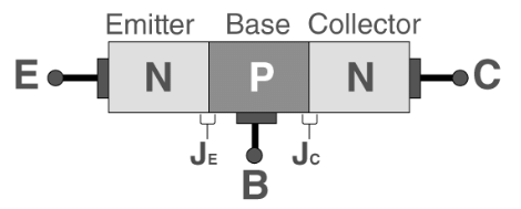
A bipolar junction transistor (BJT) is a three-terminal semiconductor device composed of two p-n junctions. It is a current-controlled device capable of amplifying current: a small change in base current produces a much larger change in collector current. The three terminals are the base (B), collector (C) and emitter (E).
- A small amplitude input signal applied at the base can be amplified and observed at the collector, provided a suitable DC power supply biases the transistor.
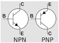
- BJTs are available in two polarities: NPN and PNP, differing in the doping arrangement of the three regions.
- Typical applications include amplifiers, switches, oscillators and many analogue and digital circuits.
Construction of a Bipolar Junction Transistor
A BJT is formed by joining three doped semiconductor regions: the emitter, base and collector. The emitter is heavily doped to inject carriers, the base is very thin and lightly doped to allow carriers to diffuse through, and the collector is moderately doped and larger to collect carriers and dissipate heat.
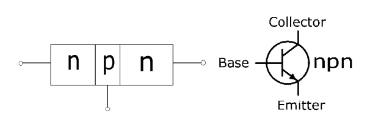
- NPN transistor: an n-type emitter and collector with a thin p-type base between them.
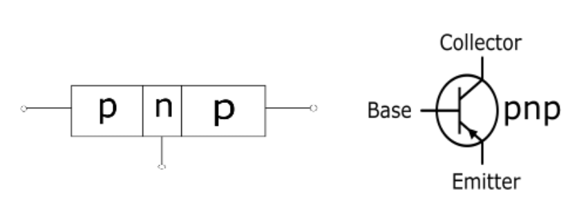
- PNP transistor: a p-type emitter and collector with a thin n-type base between them.
- The two p-n junctions are the emitter-base (E-B) junction and the collector-base (C-B) junction.
Try yourself: Which one is not the terminals of a transistor?
Modes of Operation & Biasing
Biasing means applying DC voltages to the transistor terminals. By choosing the polarities of the emitter-base and collector-base junctions we get different modes of operation:
- Active mode: Emitter-base junction forward biased and collector-base junction reverse biased. This is the normal operating region for amplification.
- Saturation mode: Both emitter-base and collector-base junctions forward biased. The transistor is fully ON and acts like a closed switch.
- Cutoff mode: Both emitter-base and collector-base junctions reverse biased. The transistor is fully OFF and acts like an open switch.
- Inverse (or inverted) mode: Emitter-base junction reverse biased and collector-base junction forward biased. The transistor does not perform as intended in normal circuits and is not used practically for amplification.

Operating Regions
- Active region: Used for linear amplification; collector current depends primarily on base current and collector-emitter voltage must keep C-B junction reverse biased.
- Saturation region: Transistor fully ON; further increase in base drive produces little increase in collector current; VCE is small (sat. voltage).
- Cutoff region: Transistor fully OFF; collector current is approximately zero (leakage currents aside).
Types of Bipolar Junction Transistor
- PNP BJT
- NPN BJT
1. PNP BJT
In a PNP transistor the base is n-type and the emitter and collector are p-type. Conventional current flows from emitter → base → collector when the emitter-base junction is forward biased and the collector-base junction is reverse biased.
2. NPN BJT
In an NPN transistor the base is p-type and the emitter and collector are n-type. Conventional current flows from collector → emitter when the emitter-base junction is forward biased and the collector-base junction is reverse biased.
Function and Carrier Transport
- BJTs rely on diffusion of charge carriers: majority carriers injected from the emitter diffuse across the thin base and are collected by the collector.
- The emitter is heavily doped to provide a large injection of carriers; the base is thin and lightly doped to allow most injected carriers to reach the collector.
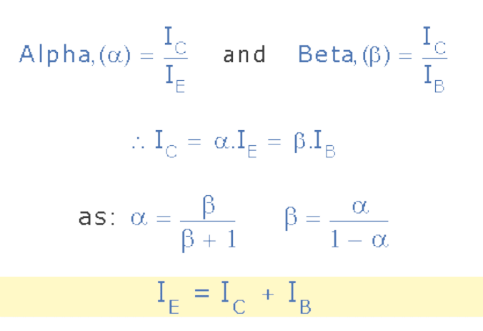
- Typical relationship between terminal currents is Ie = Ic + Ib, where Ie is emitter current, Ic collector current and Ib base current.
Voltage, Charge-Control and Current Relations
- The collector current is controlled by the base-emitter voltage through the transistor's charge distribution and recombination in the base region.
- Simple current-gain parameters are defined as α and β:
α = Ic / Ie
β = Ic / Ib
- These parameters are related by β = α / (1 - α) and equivalently α = β / (β + 1).
- Typical values of β for general-purpose transistors lie between about 20 and 200; α is always less than unity (typically 0.98-0.995).
- Transistor behaviour is also modelled by charge-control models (for example the Glenn poon model mentioned in some texts) that describe charge storage and transient effects.
Configurations of a BJT
Because a BJT has three terminals, there are three standard amplifier configurations. In each configuration one terminal is common to both input and output:
- Common emitter (CE): Base is input, collector is output, emitter is common. Provides both voltage and current gain and is the most widely used amplifier configuration.
- Common collector (CC) or emitter follower: Base is input, emitter is output, collector is common. Provides current gain but voltage gain ≲ 1; used for impedance matching.
- Common base (CB): Emitter is input, collector is output, base is common. Provides voltage gain but current gain ≲ 1; used where low input impedance and high-frequency response are required.
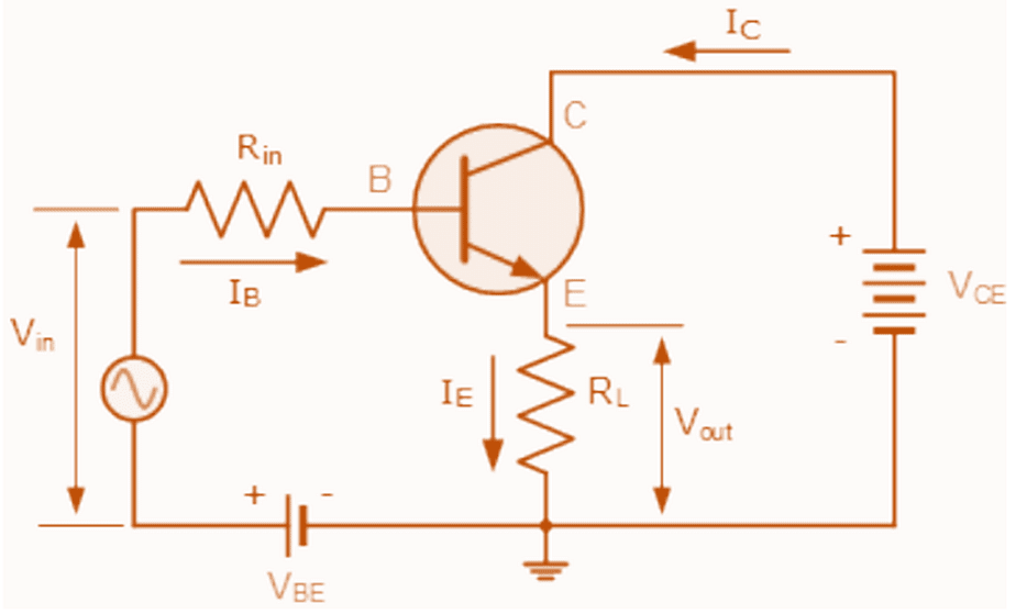
The Common Emitter (CE) Configuration
- In the common emitter configuration the input is applied between base and emitter and the output is taken between collector and emitter.
- This configuration gives significant current gain and power gain, and substantial voltage gain in many amplifier designs.
- Input impedance is relatively low (because the input sees a forward-biased base-emitter junction) and output impedance is relatively high (because the collector is taken from a reverse-biased junction).
- The CE amplifier is an inverting amplifier: the output is approximately 180° out of phase with the input.
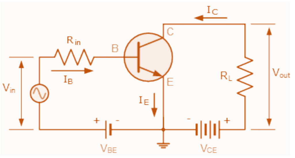
- The terminal currents obey Ie = Ic + Ib.
- The current gain of a transistor is β = Ic / Ib; the ratio α = Ic / Ie.
- Typical β values range from 20 to 200 for many small-signal transistors, so a small change in base current produces a much larger change in collector current.
- In summary, the CE configuration has high current and power gain, moderate input impedance and high output impedance, and is widely used for voltage amplification where phase inversion is acceptable.
Try yourself: For common emitter configuration, which of the following is the correct relation?
The Common Collector (CC) Configuration (Emitter Follower)
- In the common collector the collector is common to both input and output (usually tied to the supply). The input is at the base and the output is taken from the emitter.
- This arrangement is commonly called an emitter follower or voltage follower because Vout ≈ Vin - VBE, where VBE ≈ 0.7 V for silicon transistors.
- The emitter follower has very high input impedance and low output impedance, making it ideal for impedance matching between a high-impedance source and a low-impedance load.
The load is connected in series with the emitter so the emitter current flows through the load. Since emitter current is approximately the sum of collector and base currents, the stage provides a large current gain while the voltage gain is always less than unity.
The Common Collector Current Gain
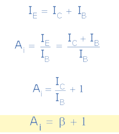
The CC configuration is a non-inverting buffer: Vin and Vout are in phase. It offers excellent current amplification and voltage buffering but little voltage gain.
The Common Base (CB) Configuration
- In the common base the base terminal is common (often grounded) to both input and output. The input is applied to the emitter and the output is taken from the collector.
- The CB configuration typically has low input impedance and high output impedance. The current gain is approximately unity or slightly less (Ic < ie),="" so="" it="" is="" not="" used="" when="" current="" amplification="" is="">
- The CB stage provides good voltage gain and is non-inverting (Vin and Vout are in phase).
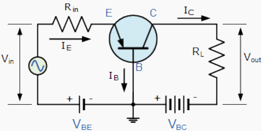
- Because the emitter injects carriers directly to the base-collector region, the input behaviour of a CB amplifier resembles that of a forward-biased diode while the output reflects the collector characteristics.
- The CB configuration is used where low input impedance and wide bandwidth are needed, for example in certain RF amplifier stages.
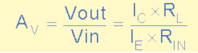
Common Base Voltage Gain:
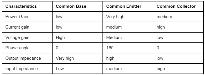
Comparison of Configurations
The main characteristics of the three configurations (input impedance, output impedance, current gain, voltage gain, phase relation) are commonly summarised together for quick comparison.
Applications of BJT
BJTs are versatile and widely used in analogue and digital electronics. Typical applications include:
- Amplifiers: Audio, RF and intermediate-frequency amplifiers using CE, CB or CC stages as required.
- Switches: Saturation and cutoff regions are used to implement electronic switching in digital logic and power control.
- Oscillators: Active elements in sine-wave and relaxation oscillators.
- Detectors / Demodulators: Used in AM/FM demodulation and other signal-detection tasks.
- Clipping and Clamping circuits: Wave shaping and level-limiting using transistor conduction thresholds.
- Impedance matching: Emitter followers (CC) provide buffering between stages with very different impedances.
- Logic circuits: Bipolar transistors form the basis of many TTL and discrete logic implementations.
Summary
A BJT is a three-terminal, current-controlled device used principally for amplification and switching. Understanding its construction, biasing modes (active, saturation, cutoff), terminal current relations (Ie = Ic + Ib; α and β) and the three basic configurations (CE, CC, CB) is essential for designing and analysing analogue circuits. Each configuration has distinct input/output impedance, gain and phase characteristics that determine its suitable applications.
FAQs on Basics of BJT
| 1. What is a Bipolar Junction Transistor (BJT)? |  |
| 2. What are the modes of operation and characteristics of a BJT? | |
| 3. What is the configuration of a Bipolar Junction Transistor? | |
| 4. What are the basics of BJT electronics and communication engineering? | |
| 5. What are some frequently asked questions about BJT? | |


|
Explore Courses for Electronics and Communication Engineering (ECE) exam
|
|

|
Get EduRev Notes directly in your Google search
|
|