Energy Bands and Generation Of Carriers Gate Questions | Electronic Devices - Electronics and Communication Engineering (ECE) PDF Download
Q.1. At T = 300 K, the band gap and the intrinsic carrier concentration of GaAs are 1.42 eV and 106 cm-3 respectively. In order to generate electron hole pairs in GaAs, which one of the wavelength (λc) ranges of incident radiation, is most suitable? (Given that: Plank’s constant is 6.62 x 10⁻³⁴ J-s velocity of light is 3 x 1010 cm/s and charge of electron is 1.6 x 10⁻¹⁹ C)
(a) 0.42 μm < λc < 0.87 μm
(b) 0.87 μm < λc < 1.42 μm
(c) 1.42 μm < λc < 1.62 μm
(d) 1.62 μm < λc < 6.62 μm
Correct Answer is Option (a)
Energy of each photon in radiation is given by,
Now, since energy required is more than band gap and energy is inversely proportional to wavelength.
Therefore, λ < 0.87μm
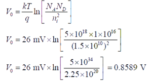
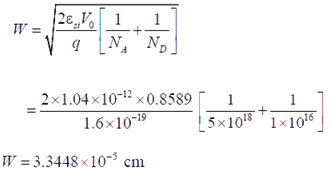
Q.2. The donor and accepter impurities in an abrupt junction silicon diode are 1 x 1016 cm-3 and 5 x 1018 cm-3, respectively. Assume that the intrinsic carrier concentration in silicon ni = 1.5 x 1010 cm-3 at 300K, kT/q = 26 mV and the permittivity of silicon  The built-in potential and the depletion width of the diode under thermal equilibrium conditions, respectively, are
(a) 0.7 V and 1 x 10⁻⁴ cm
(b) 0.86 V and 1 x 10⁻⁴ cm
(c) 0.7 V and 3.3 x 10⁻⁵ cm
(d) 0.86 V and 3.3 x 10⁻⁵ cm
Correct Answer is Option (d)
Intrinsic carries concentration,
Build in potential of a p-n junction diode is given by
Depletion width of a p-n junction diode is given by
Q.3. A thin P-type silicon sample is uniformly illuminated with light which generates excess carriers. The recombination rate is directly proportional to
(a) The minority carrier mobility
(b) The minority carrier recombination lifetime
(c) The majority carrier concentration
(d) The excess minority carrier concentration
Correct Answer is Option (d)
Recombination rate,= Electron and hole concentrations respectively under thermal equilibrium
nn and pn = Excess elements and hole concentrations respectively
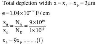
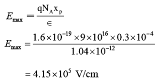
Q.4. When a silicon diode having a doping concentration of NA = 9 × 1016 cm-3 on p-side and ND = 1 × 1016 cm-3 on n-side is reverse biased, the total depletion width is found to be 3μm. Given that the permittivity of silicon is 1.04 × 10⁻¹² F/cm, the depletion width on the p-side and the maximum electric field in the depletion region, respectively, are
(a) 2.7 μm and 2.3 × 10⁵ V/cm
(b) 0.3 μm and 4.15 × 10⁵ V/cm
(c) 0.3 μm and 0.42 × 10⁵ V/cm
(d) 2.1 μm and 0.42 × 10⁵ V/cm
Correct Answer is Option (b)
Given:
NA = 9 × 10¹⁶/cm3
ND = 1016/cm3
The maximum electric field occur at the junction.
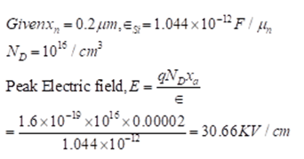
Q.5. Consider an abrupt PN junction (at T = 300 K) shown in the figure. The depletion region width Xn on the N-side of the junction is 0.2 μm and the permittivity of silicon (εsi) is 1.044 x 10⁻¹² F/cm At the junction, the approximate value of the peak electric field (in kV/cm) is _________.
 (a) 25.40
(b) 28.32
(c) 30.66
(d) 32.42
Correct Answer is Option (c)
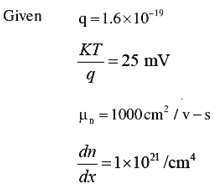
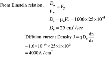
Q.6. Assume electronic charge q = 1.6 × 10⁻¹⁹ C, kT/q = 25 mV and electron mobility μn = 1000 cm2/V-s. If the concentration gradient of electrons injected into a P-type silicon sample is 1 × 10²¹/cm4, the magnitude of electron diffusion current density (in A/cm2) is _________.
(a) 2000 A/cm2
(b) 4000 A/cm2
(c) 6000 A/cm2
(d) 8000 A/cm2
Correct Answer is Option (a)
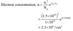
Q.7. The doping concentrations on the p-side and n-side of a silicon diode are 1 x 1016cm-3 and 1 x 1017cm−3, respectively. A forward bias of 0.3 V is applied to the diode. At T = 300K, the intrinsic carrier concentration of silicon ni = 1.5 x 1010cm-3 and kT/q = 26mV. The electron concentration at the edge of the depletion region on the p-side is
(a) 2.3 x 109cm-3
(b) 1 x 1016cm-3
(c) 1 x 1017cm-3
(d) 2.25 x 106cm-3
Correct Answer is Option (a)
Given the doping concentration on p-side
NA = 1 x 1016 cm-3
Forward bias voltage, V = 0.3 V
Intrinsic carrier concentration,
ni = 1.5 x 1010cm-3
Thermal voltage,
So, the equilibrium electron concentration on the p-side is
Q.8. An n-type silicon sample is uniformly illuminated with light which generates 1020 electron hole pairs per cm3 second. The minority carrier lifetime in the sample is 1 μs. In the steady state, the hole concentration in the sample is approximately 10x, where x is an integer. The value of x is_______.
(a) 4
(b) 14
(c) 2
(d) 12
Correct Answer is Option (b)
- Rate of generation =1020 electron-hole pairs per cm3 per second.
- At steady state (at the end of lifetime) t = 1μsec, concentration of hole-electron pair in 1 μsec is
= 1020 × 10–6 = 1014
So, x = 14
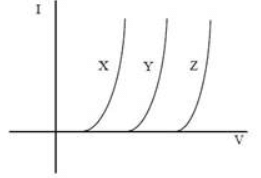
Q.9. The I-V characteristics of three types of diodes at room temperature made of semiconductors X, Y, and Z, are shown in the figure. Assume that the diodes are uniformly doped and identical in all respects except their materials. If EgX, EgY, and EgZ are the band gaps of X, Y, and Z, respectively, then
 (a) EgX > EgY > EgZ
(b) EgX = EgY = EgZ
(c) EgX < EgY < EgZ
(d) no relationship among these band gaps exists
Correct Answer is Option (c)
The current through a diode is given by:
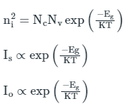
Va = Applied forward voltageIs = Saturation current given by the expression:
pn0 and np0 are the minority carrier concentration of holes and electrons respectively given by:
Also, the intrinsic carrier concentration ni is related to the Energy bandgap as:
Thus for greater Eg (bandgap), I0 will be less at a given bias.∴ EgX < EgY < EgZ
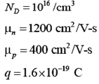
Q.10. A silicon sample is uniformly doped with donor type impurities with a concentration of 1016/cm3. The electron and hole mobilities in the sample are 1200 cm2/V-s and 400 cm2/V-s respectively. Assume complete ionization of impurities. The charge of an electron is 1.6 × 10⁻¹⁹C. The resistivity of the sample (in Ω-cm) is _______
Ans. 0.52
Given,
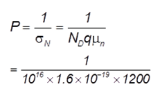
Resistivity of a semi conductor is given by
= 0.52 Ω-cm
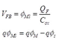
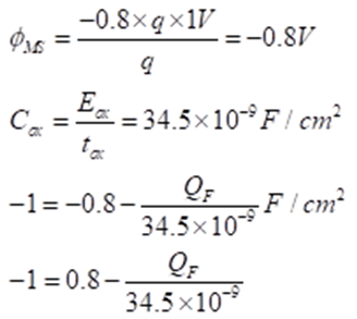
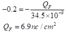
Q.11. A MOS capacitor is fabricated on p-type Si (Silicon) where the metal work function is 4.1 eV and electron affinity of Si is 4.0 eV. EC - EF = 0.9 eV, where EC and EF are the conduction band minimum and the Fermi energy levels of Si, respectively. Oxide ϵr = 3.9, ϵo = 8.85 × 10⁻¹⁴ F/cm, oxide thickness tox = 0.1 μm and electronic charge q = 1.6 × 10⁻¹⁹ C. If the measured flat band voltage of this capacitor is -1 V, then the magnitude of the fixed charge at the oxide-semiconductor interface, in nC/cm2, is ________.
Ans. 6.85 - 6.95
Q.12. Red (R), Green (G) and Blue (B) Light Emitting Diodes (LEDs) were fabricated using p-n junctions of three different inorganic semiconductors having different band-gaps. The built-in voltages of red, green and blue diodes are VR, VG and VB, respectively. Assume donor and acceptor doping to be the same (NA and ND, respectively) in the p and n sides of all the three diodes.
Which one of the following relationships about the built-in voltages is TRUE?
(a) VR > VG > VB
(b) VR < VG < VB
(c) VR = VG = VB
(d) VR > VG < VB
Correct Answer is Option (b)
- For LED and emitting lights if Red, Blue and Green colours, doping concentration on both sides are equal.
- We know that energy band gap and built in potential of a p-n junction is inversely proportional to wavelength, i.e.
Energy gap,
Hence, as λ increases, the bandgap, and the build-in potential decreases, i.e.For λR > λG > λB, the bandgap of the respective diodes will be:
⇒ VR < VG < VB
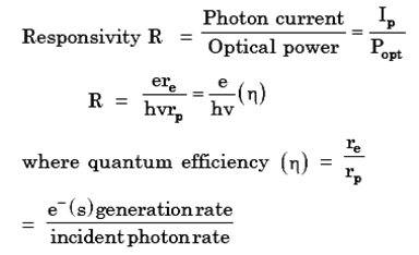
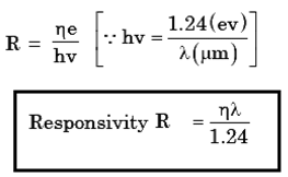
Q.13. The quantum efficiency (η) and responsivity (R) at wavelength λ (in μm) in a p-i-n photodetector are related by
(a) 
(b) 
(c) 
(d) 
Correct Answer is Option (b)
Q.14. Which one of the following options describes correctly the equilibrium band diagram at T = 300 K of a Silicon pnn+p++ configuration shown in the figure?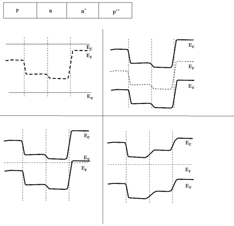 (a)
(a) 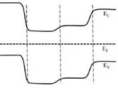
(b) 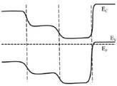
(c) 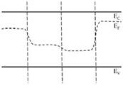
(d) 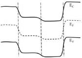
Correct Answer is Option (b)
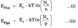
Fermi level for n & p type semiconductor are given by
EF = Fermi level
Ec - Conduction band energy
Ev - Valence band energy
Nc - Density of conduction states
Nv — Density of valence states
n - electron density
p — Hole density
from (i) As n increass Ef(n) moves closer to Ec and from (ii), as p increase Ef(p) moves closer to Ev. So fermi level must get closer to Ev for p type and to Ec for n type.
|
43 docs|29 tests
|


