Short Notes: Clipping Clamping Circuit | Analog and Digital Electronics - Electrical Engineering (EE) PDF Download
| Table of contents |

|
| Introduction |

|
| Positive Clipper |

|
| Negative Clipper |

|
| Biased Clipper |

|
| Biased Negative Clipper |

|
| Combination Clipper |

|
| Application of Clippers |

|
| Clamping Circuit |

|
| Positive Clamper |

|
| Negative Clamper |

|
Introduction
The circuit with which the applied waveform is shaped by removing or clipping a portion of that wave is known as a clipping circuit. It is also known as a limiter.- Positive Clipper
- Biased Clipper
- Combination Clipper
Positive Clipper
A positive clipper is that which removes the positive half-cycles of the input voltage.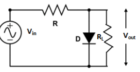
Circuit Action
During the positive half cycle of the input voltage, the diode is forward biased and conducts heavily.
Therefore, the voltage across the diode, which behaves as a short, is zero.
And hence, voltage across the load RL is zero.
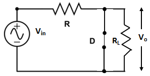 During the negative half cycle of the input voltage, the diode is reverse biased and behaves as an open.
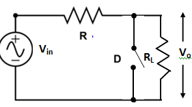
In this condition, the circuit behaves as a voltage divider with an output given by :
Generally, RL is much greater than R. So,
Input-Output Waveform
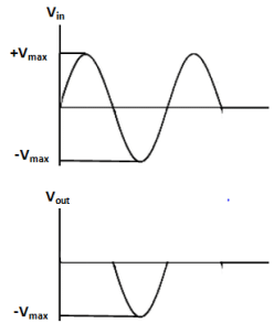
Fig.3 shows the input-output waveforms of a positive clipper. As shown, the output voltage has all the positive half cycles removed or clipped off.
Negative Clipper
If it is desired to remove the negative half cycle of the input, the only thing to be done is to reverse the polarities of the diode in the circuit shown in fig 1. Such a clipper is known as negative clipper.Biased Clipper
Sometimes, it is desired to remove a small portion of positive or negative half cycle of the signal voltage. For this purpose, biased clipper is used.
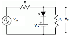
It consists of a diode D with a battery of Vdc volts.
With the polarities of the battery shown in Fig.4, a portion of each positive half cycle will be clipped off. However, the negative half cycles, will appear as such across the load, Such a clipper is called biased positive clipper.
Circuit Action
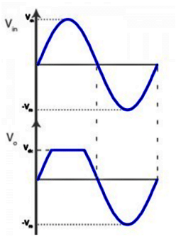
During the positive half-cycle, so long as the input voltage is greater than +Vdc, the diode will conduct heavily.
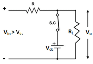
When the input voltage is greater than +V, the diode is forward biased and behaves as a short and the output voltage equals to +Vdc.
The output will stay at +Vdc, so long as the input voltage is greater than +Vdc.
During the period the input voltage is less than +Vdc, the diode is reverse biased and behaves as an open. Therefore, most of the input voltage appears across the output.
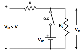
In this way the biased positive clipper removes input voltage, above +Vdc.
During the negative half cycle of the input voltage, the diode remains reverse biased. Therefore, almost entire negative half cycle appears across the load. i.e.
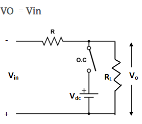
Input-Output Waveform
Fig.6 shows the input-output waveforms of a positive biased clipper. As shown, the biased positive clipper removes input voltage above +Vdc.
Biased Negative Clipper
If it is desired to clip a portion of negative half cycle of input voltage, the only thing to be done is to reverse the polarities of diode or battery. Such a circuit is known as biased negative clipper.
Combination Clipper
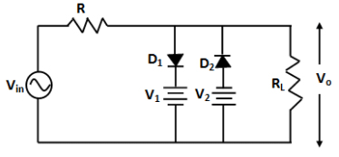
It is a combination of biased positive and negative clippers.With a combination clipper, a portion of both positive and negative half cycles of input voltage, can be removed or clipped off. The circuit diagram of a combination clipper is shown in fig.7.
Circuit Action
During the positive half cycle, so long as the positive input voltage is greater than +V1, diode D1 conducts heavily, so acts as a short while diode D2 remains reverse biased, so acts as an open as shown in fig.8(i).
Fig.8(i)
Therefore, a voltage +V1 appears across the load.
This output stays at +V1 so long as the input voltage exceeds + V1.
On the other hand, during the negative half cycle, the diode D2 will conduct heavily, and acts as a short, whereas, due to reverse bias diode D1 acts as an open and the output stays at – V2 so long as the input voltage is greater than – V2. This situation is illustrated in fig.8 (ii).
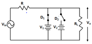
Fig.8(ii)
Note that, + V1 and – V2 are less than, +Vmax and –Vmax respectively.
Between +V1 and –V2, neither diode is on, so both the diodes D1 and D2 act as open, therefore, in this condition, most of the input voltage appears across the load as shown in fig.8(iii).
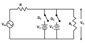
Fig.8(iii)
Input-Output Waveform
Fig.9 shows the input-output waveforms of a combination clipper.
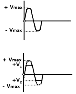
Fig.9
Application of Clippers
Clippers are used to perform one of the following two functions:
- Changing the shape of a waveform
- Circuit transient protection
- Changing the shape of waveform
- Clippers can alter the shape of a waveform.
For example, a clipper can be used to convert a sine wave into rectangular wave, square wave etc.
They can limit either positive or negative alteration or both alterations of an a.c. voltage.
Circuit Transient Protection
- A transient is a sudden current or voltage rise that has an extremely short duration.
- It can cause considerable damage to many types of circuits e.g. , a digital circuit.
- In such cases, a clipper diode can be used to prevent the transient from reaching that circuit.
Clamping Circuit
A circuit that places either the positive or negative peak of a signal at a desired d.c. level is known as a clamping circuit.

Fig.10
A clamping circuit or a camper essentially adds a d.c. component to the signal.
Fig.10 shows the key idea behind clamping.
The input signal is a sine wave having peak to peak value of 10 V.
The clamper adds the d.c. component and pushes the signal upward so that the negative peaks falls on the zero level.
It may be noted that the shape of the original signal has not changed; only there is a vertical shift in the signal. Such a clamper is known as positive clamper.
The negative clamper dos the reverse i.e. it pushes the signal downwards so that the positive peaks falls on the zero level.
The following points may be noted carefully:
- The clamping circuit does not change the peak-to-peak or r.m.s. value of the waveform.
- A clamping circuit changes the peak value and average value of a waveform.
- In the above circuit, it is easy to see that input waveform has a peak value of 5 V and average value over a cycle is zero. The clamped output varies between 10 V and 0 V. Therefore, the peak value of camped output is 10 V. And

Positive Clamper
Fig.11 shows the circuit diagram of a positive clamper.

Fig.11
The input signal is assumed to be a square wave with time period T.
The clamped output is obtained across RL.
The circuit design incorporates two main features. Firstly, the value of C and RL are so selected that time constant τ = C RL is very large.
This means that voltage across the capacitor will not discharge significantly during the interval the diode is non-conducting.
Secondly, RL C time constant is deliberately made much greater than the time period T of the incoming signal.
Operation
During the negative half cycle of the input signal, the diode is forward biased.Therefore, the diode behaves as a short as shown in fig.12.
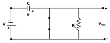
Fig.12
The charging time constant ( = CRf, where Rf = forward resistance of the diode) is very small so that the capacitor will charge to V volts very quickly.
It is easy to see that during this interval, the output voltage is directly across the short circuit.
Therefore, Vout = 0.
When the input switches to positive half cycle, the diode is reverse biased and behaves as an open as shown in fig 13.
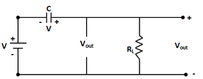
Fig.13
Since the discharging time constant (= CRL) is much greater than the time period of the input signal, the capacitor remains almost fully charged to V volts during the off time of the diode.
Now applying Kirchhoff’s voltage law to the input loop:
The resulting waveform is shown in fig.14.
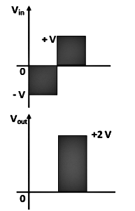
Fig.14
It is clear from the fig.14 that it is a positively clamped output. That is the input signal is pushed upward by V volts so that negative peaks fall on the zero level.
Negative Clamper
Fig.15 shows the circuit of a negative clamper.

The clamped output is taken across RL. The only change from the positive clamper is that the connections of diode are reversed.
Operation
During the positive half cycle of the input signal, the diode is forward biased.
Therefore, the diode behaves as a short as shown in fig.16.
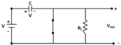
Fig.16
The charging time constant ( = CRf) is very small so that the capacitor will charge to V volts very quickly.
It can be seen that during this interval, the output voltage is directly across the short circuit.
Therefore, Vout = 0.
When the input switches to negative half cycle, the diode is reverse biased and behaves as an open as shown in fig.17.
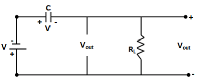
Fig.17
Since the discharging time constant (= CRL) is much greater than time period of the input signal, the capacitor almost remains fully charged to V volts during the off time of the diode.
Now applying Kirchhoff’s law to the input loop:

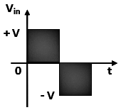
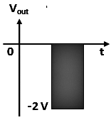
The resulting waveform is shown in fig.18. It can be noted that total swing of the output signal is equal to the total swing of the input signal.
|
135 videos|167 docs|71 tests
|
FAQs on Short Notes: Clipping Clamping Circuit - Analog and Digital Electronics - Electrical Engineering (EE)
| 1. What is a clipping circuit in electrical engineering? |  |
| 2. What is the purpose of a positive clipper in a clipping circuit? |  |
| 3. How does a negative clipper work in a clipping circuit? |  |
| 4. What is the difference between clipping and clamping circuits in electrical engineering? |  |
| 5. How can clipping circuits be used in practical applications in electrical engineering? |  |


