Previous Year Questions- Miscellaneous

Q1: Consider the OP AMP based circuit shown in the figure. Ignore the conduction drops of diodes D1 and D2. All the components are ideal and the breakdown voltage of the Zener is 5 V. Which of the following statements is true? (2023)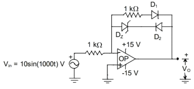
(a) The maximum and minimum values of the output voltage V0 are +15 V and -10 V, respectively.
(b) The maximum and minimum values of the output voltage V0 are +5 V and -15 V, respectively.
(c) The maximum and minimum values of the output voltage V0 are +10 V and -5 V, respectively.
(d) The maximum and minimum values of the output voltage V0 are +5 V and -10V, respectively.
Ans: (d)
Sol: During positive hall cycle:
∴ D1 → ON and D2 → OFF
Redraw the circuit :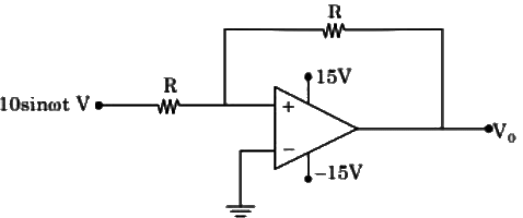 ∴ V0 = -Vi
(V0)min = -10V
During negative half cycle :
V+ > V-
Zener diode → ON, D1 → OFF and D2 → ON
Redraw the circuit: ∴ (V0)max = 5V
Q2: Two monoshot multivibrators, one positive edge triggered (M1) and another negative edge triggered (M2), are connected as shown in figure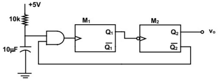 The monoshots (M1) and (M2) when triggered produce pulses of width (T1) and (T2) respectively, where (T1>T2) . The steady state output voltage (vo) of the circuit is (SET-3 (2014))
(a) 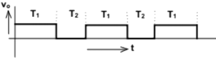 (b)
(b) 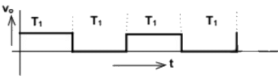 (c)
(c) 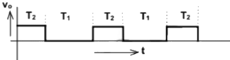 (d)
(d) 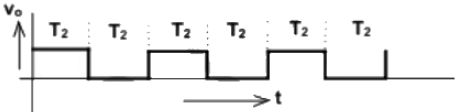 Ans: (c)
Q3: The following circuit has a source voltage Vs as shown in the graph. The current through the circuit is also shown. (2009)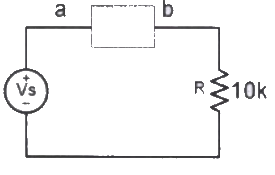
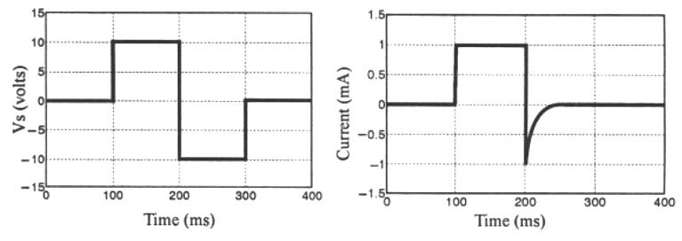 The element connected between a and b could be (2009)
(a) 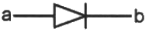 (b)
(b) 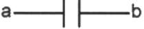 (c)
(c) 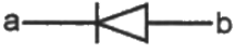 (d)
(d)  Ans: (a)
Sol: Diode act as a switch. When forward biased it is short circuited. But when suddenly reverse biased, current does not become zero instantly , initially the same current flow in opposite direction and after some time (turn off time) it will become zero.
Q4: The truth table of monoshot shown in the figure is given in the table below :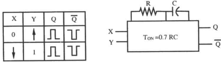 Two monoshots, one positive edge triggered and other negative edge triggered, are connected shown in the figure, The pulse widths of the two monoshot outputs Q1 and Q2 are TON1 and TON2 respectively.
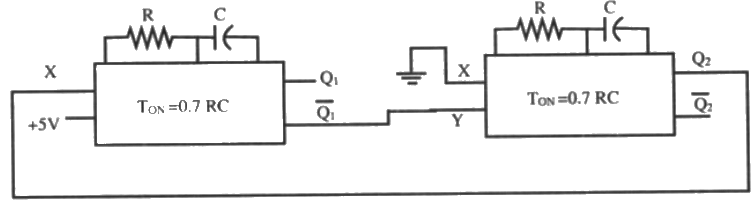 The frequency and the duty cycle of the signal at Q1 will respectively be (2008)
(a) 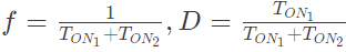
(b) 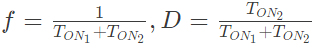
(c) 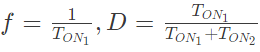
(d) 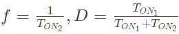
Ans: (a)
Sol: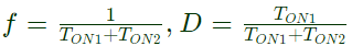
The pin description is :
1 and 8-supply;
2-trigger;
4-reset;
6-threshold
7-discharge.
The waveform appearing across the capacitor starting from t = 0, as observed on a storage CRO is (2007)
 (a)
(a)  (b)
(b) 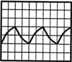 (c)
(c)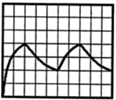 (d)
(d) 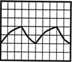 Ans: (a)
Sol: An astable multi-vibrator is providing pulse as given below
 But in this case initial voltage at capacitor is zero. So it starts from zero. Also charging time will be larger (normally) than discharging time but it is made equal by using a diode.
Q6: The input signal vin shown in the figure is a 1 kHz square wave voltage that alternates between +7 V and -7 V with a 50% duty cycle. Both transistor have the same current gain which is large. The circuit delivers power to the load resistor RL. What is the efficiency of this circuit for the given input ? choose the closest answer. (2007)
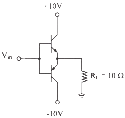 (a) 46%
(b) 55%
(c) 63%
(d) 92%
Ans: (d)
Sol: It is a class D amplifier, so η should be high η of class D amplifier is 90% to 100%.
Q7: In the Schmitt trigger circuit shown in figure, if VCE(sat) = 0.1V, the output logic low level (VOL) is (2004)
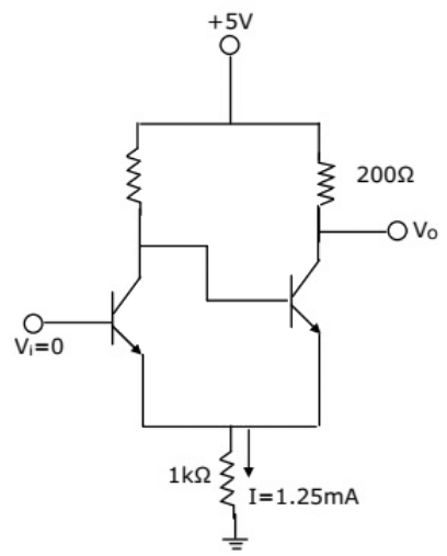 (a) 1.25 V
(b) 1.35 V
(c) 2.50 V
(d) 5.00 V
Ans: (b)
Sol: Vi = 0, then first transistor will be cut-off and current through left resistor will drive the second transistor into saturation
Then, Vo = VCE,sat + 1.25 × 10-3 × 103
= 1.35 V
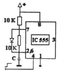
Q8: The circuit of figure shows a 555 Timer IC connected as an astable multivibrator. The value of the capacitor C is 10 nF. The values of the resistors RA and RB for a frequency of 10 kHz and a duty cycle of 0.75 for the output voltage waveform are (2003)
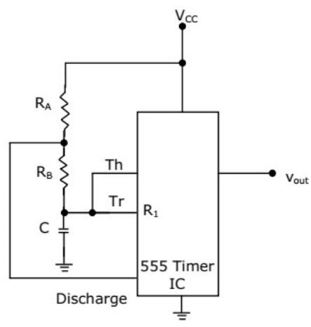 (a) RA = 3.62kΩ, RB = 3.62kΩ
(b) RA = 3.62kΩ, RB = 7.25kΩ
(c) RA = 7.25kΩ, RB = 3.62kΩ
(d) RA = 7.25kΩ, RB = 7.25kΩ
Ans: (c)
Sol: Duty cycle = α = TON/T
∴ TON = αT = 0.75 × 10-4 = 75μsec
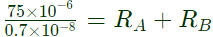 ∴ RA + RB = 10.714 kΩ
∴ TOFF = 0.7 CRB
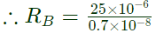 RB = 3.57kΩ, RA = 7.14kΩ
 FAQs on Previous Year Questions- Miscellaneous
| 1. What are the key topics covered in Miscellaneous Electrical Engineering exams? |  |
| 2. How can I prepare effectively for Miscellaneous Electrical Engineering questions in exams? | |
| 3. What types of questions are commonly asked in Miscellaneous Electrical Engineering exams? | |
| 4. Are there any specific formulas or theorems I should memorize for Miscellaneous Electrical Engineering? | |
| 5. What resources can I use to find previous year question papers for Miscellaneous Electrical Engineering? | |


 | Explore Courses for Electrical Engineering (EE) exam |
 | Get EduRev Notes directly in your Google search |