Depletion type MOSFET | Analog and Digital Electronics - Electrical Engineering (EE) PDF Download
| Table of contents |

|
| What is Depletion Mode MOSFET? |

|
| N-Channel Depletion MOSFET |

|
| P-Channel Depletion MOSFET |

|
| Characteristics |

|
| Drain Characteristics of N channel Depletion MOSFET |

|
| Applications |

|
What is Depletion Mode MOSFET?
A MOSFET that normally turns ON without applying any gate voltage when you connect is known as a depletion mode MOSFET. In this MOSFET, the flow of current is from the drain terminal to the source. This type of MOSFET is also known as normally on the device.
Once a voltage is applied at the gate terminal of the MOSFET, the drain to the source channel will become more resistive. When the gate-source voltage enhances more the flow of current from the drain to the source will reduce until the flow of current from the drain to the source stops.
Depletion Mode MOSFET Symbol
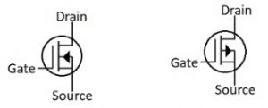
The depletion mode MOSFET symbols for p-channel and n-channel are shown below. In these MOSFETs, the arrow symbols represent the type of MOSFET like P-type or N-type. If the arrow symbol is inside direction then it is n-channel and if the arrow symbol is outside, then it is p-channel.
How Does Depletion Mode MOSFET Work?
The depletion MOSFET is activate by default. Here, source & drain terminals are connected physically. To understand the working of the MOSFET, lets understand the types of Depletion MOSFET.
Types of Depletion Mode MOSFET
The Depletion mode MOSFET structure varies based on the type. The MOSFETs are two types p-channel depletion mode and n- channel depletion mode. So, each type of depletion mode MOSFET structure and its working is discussed below.
N-Channel Depletion MOSFET
The structure of N-Channel Depletion MOSFET is shown below. In this type of depletion MOSFET, the source and drain are connected by a small strip of N-type semiconductor. The substrate used in this MOSFET is a P-type semiconductor and electrons are the majority charge carriers in this type of MOSFET. Here, the source & drain are doped heavily.
The N-channel depletion mode MOSFET construction is the same as compared to enhancement mode n channel MOSFET except its working is dissimilar. The gap between the source and drain terminals is composed of n-type impurities.
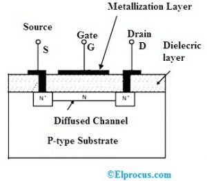
When we apply a potential difference between both the terminals like source & drain, current flows throughout the whole n-region of the substrate. When a negative voltage is applied at the gate terminal of this MOSFET, the charge carriers like electrons will get repelled & moved down within the n-region under the dielectric layer. So charge carrier depletion will occur within the channel.
Thus, the overall channel conductivity gets reduced. At this condition, once the same voltage is applied at the GATE terminal, the drain current will be decreased. Once the negative voltage is increased further it reaches the pinch-off mode.
Here the drain current is controlled by changing the depletion of charge carriers within the channel so, this is called depletion MOSFET. Here, the drain terminal is in a +ve potential, the gate terminal is in a -ve potential & the source is at ‘0’ potential. Thus the voltage variation between drain to the gate is high as compared from source to gate, so the depletion layer width is high to drain as compared to the source terminal.
P-Channel Depletion MOSFET
In the P Channel depletion MOSFET, a small strip of semiconductor of P-type connects the source and drain. The source and drain are of P-type semiconductor and the Substrate is of N-type semiconductor. The majority of charge carriers are holes.
The p channel depletion MOSFET construction is quite opposite to the n channel depletion mode MOSFET. This MOSFET includes a channel that is made in between the source & drain region which is heavily doped with p-type impurities. So, in this MOSFET, the n-type substrate is used and the channel is p-type as shown in the diagram.
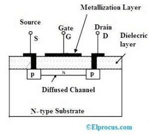
Once we apply a +ve voltage at the MOSFET’s gate terminal, then minority charge carriers like electrons in the p-type region will get attracted due to electrostatic action & form fixed negative impurity ions. So a depletion region will form within the channel & consequently, the conductivity of the channel gets reduced. In this way, the drain current is controlled by applying +ve voltage at the gate terminal.
Once we apply a +ve voltage at the MOSFET’s gate terminal, then minority charge carriers like electrons in the p-type region will get attracted due to electrostatic action & form fixed negative impurity ions. So a depletion region will form within the channel & consequently, the conductivity of the channel gets reduced. In this way, the drain current is controlled by applying +ve voltage at the gate terminal.
To activate this type of depletion type MOSFET, the gate voltage must be 0V and the drain current value is large so that the transistor will be in the active region. So, once more to turn on this MOSFET, +ve voltage is given at the source terminal. So with enough positive voltage& no voltage applied at the base terminal, this MOSFET will be in maximum operation & has a high current.
To deactivate a P-channel depletion MOSFET, there are two ways you can cut off the bias positive voltage, that powers the drain otherwise you can apply a -ve voltage to the gate terminal. Once a -ve voltage is provided to the gate terminal, the current will be decreased. As the gate voltage turns more negative, the current reduces until cutoff, then MOSFET will be in the ‘OFF’ condition. So, this stops a large source to drain current.
So, once more -ve voltage is provided to the gate terminal of this MOSFET, then this MOSFET will conduct less & less current will be there across the source-drain terminal. Once the gate voltage attains a certain –ve voltage threshold, then it turns off the transistor. So, -ve voltage turns off the transistor.
Characteristics
The drain MOSFET characteristics are discussed below.
Drain Characteristics of N channel Depletion MOSFET
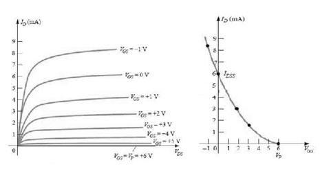
The drain characteristics of the n channel depletion MOSFET are shown below. These characteristics are plotted between the VDS and IDSS. When we keep on increasing the VDS value then the ID will increase. After a certain voltage, the drain current ID will become constant. The saturation current value for Vgs = 0 is called IDSS.
Whenever the voltage applied is negative, and then this voltage at the gate terminal will push the charge carriers like electrons to the substrate. And also holes within this p-type substrate will be attracted by these electrons. So due to this voltage, the electrons within the channel will be recombined with holes. The rate of the recombination will depend on the negative voltage applied.
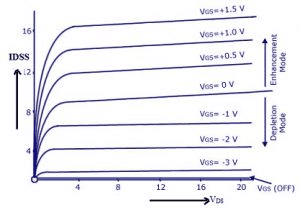
Once we increase this negative voltage, the recombination rate will also increase so which will decrease the no. of electrons available within this channel and will reduce the current flow effectively.
when we observe the above characteristics, it is seen that when the VGS value will becomes more negative then the drain current will decreases. At a certain voltage, this negative voltage will become zero. This voltage is known as pinch-off voltage.
This MOSFET also works for the positive voltage, so when we apply the positive voltage at the gate terminal then the electrons will be attracted to N-channel. So the no. of electrons within this channel will increase. So the current flow within this channel will increase. So for the positive Vgs value, the ID will be even more than IDSS.
Transfer Characteristics of N channel Depletion MOSFET
The transfer characteristics of N channel depletion MOSFET are shown below which is similar to JFET. These characteristics define the main relationship between the ID and VGS for the fixed VDS value. For the positive VGS values, we can also get the ID value.
So due to that, the curve in the characteristics will extend to the right-hand side. Whenever the VGS value is positive, the no. of electrons within the channel will increase. When the VGS is positive then this region is the enhancement region. Similarly, when the VGS is negative then this region is known as the depletion region.
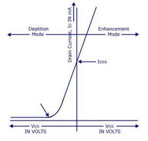
The main relationship between the ID and Vgs can be expressed through ID = IDSS (1-VGS/VP)^2. By using this expression, we can find the ID value for the Vgs.
Drain Characteristics of P channel Depletion MOSFET
The drain characteristics of P channel depletion MOSFET is shown below. Here, the VDS voltage is negative and the Vgs voltage is positive. Once we keep on increasing the Vgs then Id(drain current) will decrease. At the pinch-off voltage, this Id( drain current) will become zero. Once the VGS is negative, then the ID value will be even higher than IDSS.
Transfer Characteristics of P channel Depletion MOSFET
The transfer characteristics of P channel depletion MOSFET is shown below which is a mirror image of n channel depletion MOSFET transfer characteristics. Here we can observe that the drain current enhances in the positive VGS region from the cut-off point until IDSS, and then it continues to increase when the negative VGS value increases.
Applications
The depletion MOSFET applications include the following.
- This depletion MOSFET can be used in constant current source & linear regulator circuits as a pass transistor.
- These are extensively used in a start-up auxiliary power supply circuit.
- Normally, these MOSFETs are turned ON when no voltage is applied which means they can conduct current in normal conditions. Thus this is used in digital logic circuits as Load Resistor.
- These are used for flyback circuits within PWM ICs.
- These are used in Telecom Switches, Solid State Relays, and many more.
- This MOSFET is utilized within voltage sweeping circuits, current monitor circuits, led array driver circuits, etc.
|
211 videos|208 docs|72 tests
|


