Quantitative Theory of PN Junction Diode | Analog and Digital Electronics - Electrical Engineering (EE) PDF Download
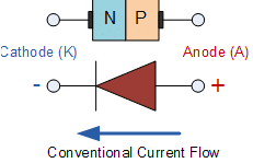
PN JUNCTION WITH NO APPLIED VOLTAGE OR OPEN CIRCUIT CONDITION:
In a piece of semiconductor, if one half is doped by p-type impurity and the other half is doped by n-type impurity, a PN junction is formed. The plane dividing the two halves or zones is called PN junction. As shown in the fig1, the N-type material has high concentration of free electrons, while P-type material has high concentration of holes. Therefore at the junction there is a tendency of free electrons to diffuse over to the P-side and the holes to the N-side. This process is called 
diffusion. As the free electrons move across the junction from N-type to P-type, the donor atoms become positively charged. Hence a positive charge is built on the N-side of the junction. The free electrons that cross the junction uncover the negative acceptor ions by filling the holes. Therefore a negative charge is developed on the P-side of the junction. This net negative charge on the P-side prevents further diffusion of electrons into the P- side. Similarly the net positive charge on the N-side repels the hole crossing from P-side to N-side. Thus a barrier is set up near the junction which prevents the further movement of charge carriers i.e. electrons and holes. As a consequence of induced electric field across the depletion layer, an electrostatic potential difference is established between P and N regions, which are called the potential barrier, junction barrier, diffusion potential or contact potential, Vo. The magnitude of the contact potential Vo varies with doping levels and temperature. Vo is 0.3V for Ge and 0.72 V for Si.
The electrostatic field across the junction caused by the positively charged N-type region tends to drive the holes away from the junction and negatively charged P-type regions tend to drive the electrons away from the junction. The majority holes diffusing out of the P region leave behind negatively charged acceptor atoms bound to the lattice, thus exposing a negative space charge in a previously neutral region. Similarly electrons diffusing from the N region expose positively ionized donor atoms and a double space charge builds up at the junction as shown in the fig. 1.7
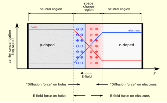
It is noticed that the space charge layers are of opposite sign to the majority carriers diffusing into them, which tends to reduce the diffusion rate. Thus the double space of the layer causes an electric field to be set up across the junction directed from N to P regions, which is in such a direction to inhibit the diffusion of majority electrons and holes as illustrated in fig 1.7. The shape of the charge density, ρ, depends upon how diode is doped. Thus the junction region is depleted of mobile charge carriers. Hence it is called depletion layer, space region, and transition region. The depletion region is of the order of 0.5µm thick. There are no mobile carriers in this narrow depletion region. Hence no current flows across the junction and the system is in equilibrium. To the left of this depletion layer, the carrier concentration is p= NA and to its right it is n= ND.
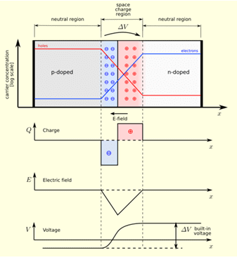 Fig. 1.8
|
137 videos|143 docs|71 tests
|
FAQs on Quantitative Theory of PN Junction Diode - Analog and Digital Electronics - Electrical Engineering (EE)
| 1. What is the quantitative theory of a PN junction diode? |  |
| 2. How does the PN junction diode work? | |
| 3. What are the important parameters in the quantitative theory of a PN junction diode? | |
| 4. How can the current-voltage characteristics of a PN junction diode be calculated using the quantitative theory? | |
| 5. What are the applications of the quantitative theory of PN junction diodes? | |

|
2.9K Views |

|
4.77/5 Rating |

|
Dec 22, 2024 Last updated |

|
Explore Courses for Electrical Engineering (EE) exam
|
|
Quantitative Theory of PN Junction Diode | Analog and Digital Electronics - Electrical Engineering (EE)
,Viva Questions
,Quantitative Theory of PN Junction Diode | Analog and Digital Electronics - Electrical Engineering (EE)
,video lectures
,shortcuts and tricks
,mock tests for examination
,Previous Year Questions with Solutions
,Extra Questions
,Objective type Questions
,ppt
,practice quizzes
,MCQs
,Free
,past year papers
,Sample Paper
,study material
,Semester Notes
,Quantitative Theory of PN Junction Diode | Analog and Digital Electronics - Electrical Engineering (EE)
,Exam
,Summary
,Important questions
;


Quantitative Theory of PN Junction Diode Free PDF Download
Importance of Quantitative Theory of PN Junction Diode
Quantitative Theory of PN Junction Diode Notes
Quantitative Theory of PN Junction Diode Electrical Engineering (EE) Questions
Study Quantitative Theory of PN Junction Diode on the App
|
© EduRev
|
Education Revolution
|


|


