Forward Biased Junction Diode | Analog and Digital Electronics - Electrical Engineering (EE) PDF Download
FORWARD BIASED JUNCTION DIODE
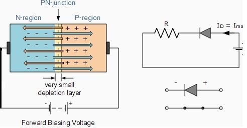
When a diode is connected in a Forward Bias condition, a negative voltage is applied to the N-type material and a positive voltage is applied to the P-type material. If this external voltage becomes greater than the value of the potential barrier, approx. 0.7 volts for silicon and 0.3 volts for germanium, the potential barriers opposition will be overcome and current will start to flow. This is because the negative voltage pushes or repels electrons towards the junction giving them the energy to cross over and combine with the holes being pushed in the opposite direction towards the junction by the positive voltage. This results in a characteristics curve of zero current flowing up to this voltage point, called the "knee" on the static curves and then a high current flows through the diode with little increase in the external voltage as shown below.
Forward Characteristics Curve for a Junction Diode

The application of a forward biasing voltage on the junction diode results in the depletion layer becoming very thin and narrow which represents a low impedance path through the junction thereby allowing high currents to flow. The point at which this sudden increase in current takes place is represented on the static I-V characteristics curve above as the "knee" point.
Forward Biased Junction Diode showing a Reduction in the Depletion Layer

This condition represents the low resistance path through the PN junction allowing very large currents to flow through the diode with only a small increase in bias voltage. The actual potential difference across the junction or diode is kept constant by the action of the depletion layer at approximately 0.3v for germanium and approximately 0.7v for silicon junction diodes. Since the diode can conduct "infinite" current above this knee point as it effectively becomes a short circuit, therefore resistors are used in series with the diode to limit the current flow. Exceeding its maximum forward current specification causes the device to dissipate more power in the form of heat than it was designed for, resulting in a quick failure of the device.
PN JUNCTION UNDER REVERSE BIAS CONDITION:
Reverse Biased Junction Diode
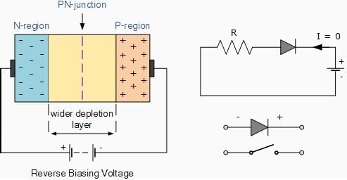
When a diode is connected in a Reverse Bias condition, a positive voltage is applied to the N-type material and a negative voltage is applied to the P-type material. The positive voltage applied to the N-type material attracts electrons towards the positive electrode and away from the junction, while the holes in the P-type end are also attracted away from the junction towards the negative electrode. The net result is that the depletion layer grows wider due to a lack of electrons and holes and presents a high impedance path, almost an insulator. The result is that a high potential barrier is created thus preventing current from flowing through the semiconductor material.
Reverse Biased Junction Diode showing an Increase in the Depletion Layer

This condition represents a high resistance value to the PN junction and practically zero current flows through the junction diode with an increase in bias voltage. However, a very small leakage current does flow through the junction which can be measured in microamperes (μA). One final point, if the reverse bias voltage Vr applied to the diode is increased to a sufficiently high value, it will cause the PN junction to overheat and fail due to the avalanche effect around the junction. This may cause the diode to short and will result in the flow of maximum circuit current, and this shown as a step downward slope in the reverse static characteristics curve below.
Reverse Characteristics Curve for a Junction Diode

Sometimes this avalanche effect has practical applications in voltage stabilising circuits where a series limiting resistor is used with the diode to limit this reverse breakdown current to a preset maximum value thereby producing a fixed voltage output across the diode. These types of diodes are commonly known as Zener Diodes and are discussed in a later tutorial.
CHARACTERISTICS AND THEIR TEMPERATURE DEPENDENCE:
Diode terminal characteristics equation for diode junction current:


Where VT = kT/q;
VD_ diode terminal voltage, Volts
Io _ temperature-dependent saturation current, µA
T _ absolute temperature of p-n junction, K
k _ Boltzmann’s constant 1.38 x 10⁻²³J/K)
q _ electron charge 1.6 x 10⁻¹⁹ C η = empirical constant, 1 for Ge and 2 for Si

Temperature Effects on Diode
Temperature can have a marked effect on the characteristics of a silicon semiconductor diode as shown in Fig. 1.24. It has been found experimentally that the reverse saturation current Io will just about double in magnitude for every 10°C increase in temperature.

It is not uncommon for a germanium diode with an Io in the order of 1 or 2 A at 25°C to have a leakage current of 100 A _ 0.1 mA at a temperature of 100°C. Typical values of Io for silicon are much lower than that of germanium for similar power and current levels. The result is that even at high temperatures, the levels of Io for silicon diodes do not reach the same high levels obtained for germanium—a very important reason that silicon devices enjoy a significantly higher level of development and utilization in design. Fundamentally, the open-circuit equivalent in the reverse bias region is better realized at any temperature with silicon than with germanium. The increasing levels of Io with temperature account for the lower levels of threshold voltage, as shown in Fig. 1.24. Simply increase the level of Io in and not rise in diode current. Of course, the level of TK also will be increased, but the increasing level of Io will overpower the smaller percent change in TK. As the temperature increases the forward characteristics are actually becoming more “ideal,”
|
137 videos|143 docs|71 tests
|
FAQs on Forward Biased Junction Diode - Analog and Digital Electronics - Electrical Engineering (EE)
| 1. What is a forward biased junction diode? |  |
| 2. How does a forward biased junction diode work? |  |
| 3. What is the purpose of forward biasing a diode? |  |
| 4. What happens if a voltage higher than the forward bias voltage is applied to a diode? |  |
| 5. Can a forward biased junction diode block current flow? |  |

|
Explore Courses for Electrical Engineering (EE) exam
|

|


