Fan Out | Digital Circuits - Electronics and Communication Engineering (ECE) PDF Download

Fan Out
A standard LS TTL gate is therefore able to sink 20 times the amount of current it is able to source. This ratio between sinking and sourcing current is typical with bipolar gates. The above conditions mean that the output of a standard LS TTL gate is capable of driving up to 20 LS TTL inputs without its output voltage falling below the minimum specified for logic 1. This is described as a FAN OUT FACTOR of 20, but each logic family has its own particular ratio of sinking to sourcing currents, so the fan out factor of 20 is only correct where a standard LS TTL gate is driving one or more gates of the same (LS TTL) family.
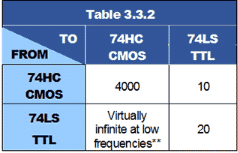
Because gates of other families have different input and output currents the actual fan out factor will be different when logic families are mixed within a circuit. For example, Table 3.3.2 shows how mixing LS TTL and CMOS HC gates affects their fan out factors.
A 74HC output can feed up to 4000 74HC inputs, because the input currents of 74HC gates are extremely low, but only 10 74LS TTL inputs.
A Standard LS TTL gate output can drive up to 20 LS TTL inputs, but one LS TTL gate output can drive a virtually infinite number of 74HC CMOS gates because of the low current requirement of 74HC CMOS gates.
High Frequency AC Fan Out **
However, although a standard LS TTL output will apparently feed an infinite number of 74HC inputs (** in Table 3.3.2), when high frequency signals are used, additional limits need to be considered. Each CMOS input and output has a capacitance of several pF, and if a CMOS output is to feed a number of inputs, the individual input capacitances are in effect connected in parallel (and so add) to form a larger capacitance across any output driving the CMOS inputs.
The effect of this capacitance, as well as any capacitance due to connecting lines on the printed circuit board will combine with the output impedance of the gate to form a low pass filter. The effect of this filter will be to remove some of the higher frequencies in the signal, increasing rise and fall times, lengthening propagation delay and potentially causing timing errors in the system, therefore large fan outs are best avoided. These effects make the design of high-speed digital systems similar in some respects to high frequency RF circuits where stray capacitance, cable routing and interference play a large part in the circuit design.
|
75 videos|188 docs|70 tests
|
FAQs on Fan Out - Digital Circuits - Electronics and Communication Engineering (ECE)
| 1. What is the TOEFL exam? |  |
| 2. How is the TOEFL exam structured? | |
| 3. How long is the TOEFL exam? | |
| 4. How is the TOEFL exam scored? | |
| 5. What is the validity of TOEFL scores? | |


study material
,practice quizzes
,past year papers
,MCQs
,Exam
,Objective type Questions
,Viva Questions
,Fan Out | Digital Circuits - Electronics and Communication Engineering (ECE)
,Fan Out | Digital Circuits - Electronics and Communication Engineering (ECE)
,Important questions
,mock tests for examination
,Extra Questions
,Summary
,Free
,Semester Notes
,Sample Paper
,Fan Out | Digital Circuits - Electronics and Communication Engineering (ECE)
,ppt
,video lectures
,shortcuts and tricks
,Previous Year Questions with Solutions
;


Fan Out Free PDF Download
Importance of Fan Out
Fan Out Notes
Fan Out Electronics and Communication Engineering (ECE) Questions
Study Fan Out on the App
|
© EduRev
|
Education Revolution
|


|


