Switch De-Bouncing: S-R Flip Flops | Analog and Digital Electronics - Electrical Engineering (EE) PDF Download

Switch De-Bouncing
The fact that repeated pulses at the  inputs are ignored after the initial pulse has set or reset the Q output, makes the SR Flip-flop useful for switch de-bouncing.
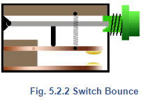
When any moving object collides with a stationary object it tends to bounce; the contacts in switches are no exception to this rule. Although the contacts may be tiny and the movement small, as the contacts close they will tend to bounce rather than close and stay closed.
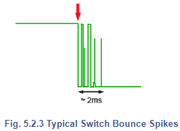
This causes a number of very fast on and off states for a short time, until the contacts stop bouncing in the closed position. The length of time of the bouncing may be very short, as shown in Fig. 5.2.3 where a number of fast pulses occur for about 2ms after the switch is initially closed (red arrow). For many applications this switch bounce may be ignored, but in digital circuits the repeated ones and zeros occurring after a switch is closed, will be recognised as additional switching actions.
Switch De-Bounce Circuit
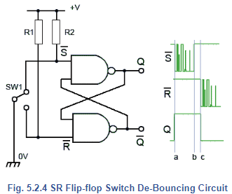
The SR flip-flop is very effective in removing the effects of switch bounce and Fig 5.2.4 illustrates how a SR flip-flop can be used to produce clean pulses using SWI, which is a ‘break before make’ changeover switch. When SW1 connects the upper contact to 0V, the S input changes from logic 1 to logic 0 and R is ‘pulled up’ to logic 1 by R1.
As soon as  is at logic 0, (at time ‘a’ in Fig. 5.2.4) output Q will be at logic 1 and any further pulses due to switch bounce will be ignored.
When SW1 is switched to the lower contact, there will be a short time (between times ‘b’ and ‘c’ in Fig. 5.2.4) when neither or  is connected to 0V. During this time returns to logic 1, therefore both inputs will be at logic 1 until time ‘c’, when SW1 connects R to 0V and Q is reset to logic 0 completing the output pulse. The use of a ‘break before make’ rather than a ‘make before break’ switch is important, as it ensures that during the changeover period (time ‘b’ to time ‘c’ in Fig. 5.2.4) both inputs are at logic 1 rather than the non-allowed state where both inputs would be logic 0. This ensures that outputs Q and
  are never at the same logic state.
Although, during the change over of SW1 both inputs are at logic 1, this does not produce the indeterminate state described in Table 5.2.1, as one or other of the inputs is always at logic 0 before both inputs become logic 1.
|
135 videos|167 docs|71 tests
|
FAQs on Switch De-Bouncing: S-R Flip Flops - Analog and Digital Electronics - Electrical Engineering (EE)
| 1. What is switch de-bouncing? |  |
| 2. How does an S-R flip flop help in switch de-bouncing? | |
| 3. What are some common de-bouncing techniques other than S-R flip flops? | |
| 4. Why is switch de-bouncing important in digital circuits? | |
| 5. Can switch de-bouncing be necessary for all types of switches? | |


mock tests for examination
,Switch De-Bouncing: S-R Flip Flops | Analog and Digital Electronics - Electrical Engineering (EE)
,Switch De-Bouncing: S-R Flip Flops | Analog and Digital Electronics - Electrical Engineering (EE)
,video lectures
,Free
,Summary
,Previous Year Questions with Solutions
,practice quizzes
,Objective type Questions
,study material
,Viva Questions
,Sample Paper
,MCQs
,past year papers
,ppt
,shortcuts and tricks
,Extra Questions
,Switch De-Bouncing: S-R Flip Flops | Analog and Digital Electronics - Electrical Engineering (EE)
,Semester Notes
,Exam
,Important questions
;


Switch De-Bouncing: S-R Flip Flops Free PDF Download
Importance of Switch De-Bouncing: S-R Flip Flops
Switch De-Bouncing: S-R Flip Flops Notes
Switch De-Bouncing: S-R Flip Flops Electrical Engineering (EE) Questions
Study Switch De-Bouncing: S-R Flip Flops on the App
|
© EduRev
|
Education Revolution
|


|


