Electrical Engineering (EE) Exam  >  Electrical Engineering (EE) Test  >  Analog and Digital Electronics  >  Test: DC Imperfections in Operational Amplifiers - Electrical Engineering (EE) MCQ

DC Imperfections in Operational Amplifiers - GATE EE Analog and Digital


MCQ Practice Test & Solutions: Test: DC Imperfections in Operational Amplifiers (10 Questions)

You can prepare effectively for Electrical Engineering (EE) Analog and Digital Electronics with this dedicated MCQ Practice Test (available with solutions) on the important topic of "Test: DC Imperfections in Operational Amplifiers". These 10 questions have been designed by the experts with the latest curriculum of Electrical Engineering (EE) 2026, to help you master the concept.

Test Highlights:

  • - Format: Multiple Choice Questions (MCQ)
  • - Duration: 10 minutes
  • - Number of Questions: 10

Sign up on EduRev for free to attempt this test and track your preparation progress.

Test: DC Imperfections in Operational Amplifiers - Question 1

Consider an inverting amplifier with a nominal gain of 1000 constructed from an op amp with an input offset voltage of 3 mV and with output saturation levels of ±10 V. What is (approximately) the peak sine-wave input signal that can be applied without output clipping?

Detailed Solution: Question 1

The maximum that can be sent without clipping is 10V – 1000 X 3mV or 7V.

Test: DC Imperfections in Operational Amplifiers - Question 2

(Q2 & Q.3) Consider an inverting amplifier with a nominal gain of 1000 constructed from an op amp with an input offset voltage of 3 mV and with output saturation levels of ±10 V. If the effect of VOs(input offset voltage) is nulled at room temperature (250C), how large an input can one now apply if:
Q. The circuit is to operate at a constant temperature?

Detailed Solution: Question 2

 Explanation: Maximum signal that will not be clipped is 10mV because 10mV X 1000 = 10V.

Test: DC Imperfections in Operational Amplifiers - Question 3

The circuit is to operate at a temperature in the range 0°C to 75°C and the temperature coefficient of VOS is 10 μV/°C?

Detailed Solution: Question 3

Since the effect is nullified at 25oC, the peak that can be sent now is given by 10 – (75-25) X 0.1 mV.

Test: DC Imperfections in Operational Amplifiers - Question 4

One of the DC imperfections of the amplifiers are dc offset voltage which is

Detailed Solution: Question 4

DC offset voltage is existence of output signal even when the differential signal is zero.

Test: DC Imperfections in Operational Amplifiers - Question 5


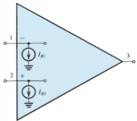
For the amplifier shown determine the value of the bias current (Ib) and input offset current (Io) respectively.

Detailed Solution: Question 5

Standard mathematical expressions are used with the given variables.

Test: DC Imperfections in Operational Amplifiers - Question 6

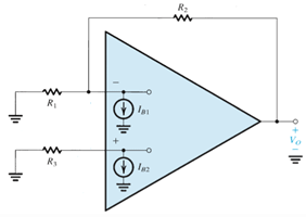
Consider the circuit shown below which reduces the impact of the input bias current. If IB1 = IB2 = Input bias current, then determine the value of R3 so that the output voltage (v0) is not impacted by the input bias current.

Detailed Solution: Question 6

This will be possible when R3 has the same value as the net effect of R1 and R2.

Test: DC Imperfections in Operational Amplifiers - Question 7

Consider an inverting amplifier circuit designed using an op amp and two resistors, R1 = 10 kΩ and R2 = 1 MΩ. If the op amp is specified to have an input bias current of 100 nA and an input offset current of 10 nA, find the output dc offset voltage resulting.

Detailed Solution: Question 7

Use the mathematical definition of bias current and offset current.

Test: DC Imperfections in Operational Amplifiers - Question 8

(Q.8-Q.10) Consider a Miller integrator with a time constant of 1ms and an input resistance of 10 kΩ. Let the op amp have VOS (offset voltage) = 2 mV and output saturation voltages of ±12 V.​

Q. Assuming that when the power supply is turned on the capacitor voltage is zero, how long does it take for the amplifier to saturate?

Detailed Solution: Question 8

 Use vO = VOS
(VOS/CR)t.

Test: DC Imperfections in Operational Amplifiers - Question 9

Select the largest possible value for a feedback resistor RF so that at least ±10 V of output signal swing remains available.

Detailed Solution: Question 9

Use vO = VOS
(VOS/CR)t.

Test: DC Imperfections in Operational Amplifiers - Question 10

What is the corner frequency of the resulting STC network?

Detailed Solution: Question 10

 The required answer is given by 1/6 Hz.

135 videos|182 docs|71 tests
Information about Test: DC Imperfections in Operational Amplifiers Page
In this test you can find the Exam questions for Test: DC Imperfections in Operational Amplifiers solved & explained in the simplest way possible. Besides giving Questions and answers for Test: DC Imperfections in Operational Amplifiers, EduRev gives you an ample number of Online tests for practice
135 videos|182 docs|71 tests
Download as PDF