NEET Exam  >  NEET Test  >   Past Year Papers  >  31 Year NEET Previous Year Questions: Semiconductor Electronics - 4 - NEET MCQ

31 Year NEET Previous Questions: Semiconductor Electronics - 4 Free MCQ


MCQ Practice Test & Solutions: 31 Year NEET Previous Year Questions: Semiconductor Electronics - 4 (25 Questions)

You can prepare effectively for NEET NEET Past Year Papers with this dedicated MCQ Practice Test (available with solutions) on the important topic of "31 Year NEET Previous Year Questions: Semiconductor Electronics - 4". These 25 questions have been designed by the experts with the latest curriculum of NEET 2026, to help you master the concept.

Test Highlights:

  • - Format: Multiple Choice Questions (MCQ)
  • - Duration: 50 minutes
  • - Number of Questions: 25

Sign up on EduRev for free to attempt this test and track your preparation progress.

31 Year NEET Previous Year Questions: Semiconductor Electronics - 4 - Question 1

p-n junction is said to be forward biased, when      [1988]

Detailed Solution: Question 1

For forward biasing of p-n junction, the
positive terminal of external battery is to be
connected to p-semiconductor and negative
terminal of battery to the n-semiconductor.

31 Year NEET Previous Year Questions: Semiconductor Electronics - 4 - Question 2

At absolute zero, Si acts as [1988]

Detailed Solution: Question 2

Semiconductors are insulators at room
temperature

31 Year NEET Previous Year Questions: Semiconductor Electronics - 4 - Question 3

When n-type semiconductor is heated [1989]

Detailed Solution: Question 3

Due to heating, when a free electron is
produced then simultaneously a hole is also
produced.

31 Year NEET Previous Year Questions: Semiconductor Electronics - 4 - Question 4

Radiowaves of constant amplitude can begenerated with [1989]

Detailed Solution: Question 4

Radiowaves of constant amplitude can be
produced by using oscillator with proper
feedback.

31 Year NEET Previous Year Questions: Semiconductor Electronics - 4 - Question 5

In a common base amplifier the phase differencebetween the input signal voltage and the outputvoltage is [1990]

Detailed Solution: Question 5

The phase difference between output
voltage and input signal voltage in common
base transistor or circuit is zero.

31 Year NEET Previous Year Questions: Semiconductor Electronics - 4 - Question 6

When a triode is used as an amplifier the phasedifference between the input signal voltage andthe output is [1990]

Detailed Solution: Question 6

Voltage gain of an amplifier

The negative sign indicates that the output
voltage differs in phase from the input
voltage by 180°(or π). This holds for a pure
resistive load.

31 Year NEET Previous Year Questions: Semiconductor Electronics - 4 - Question 7

The depletion layer in the p-n junction region iscaused by [1991]

Detailed Solution: Question 7

The depletion layer in the p-n junction region
is caused by diffusion of charge carriers.

31 Year NEET Previous Year Questions: Semiconductor Electronics - 4 - Question 8

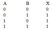
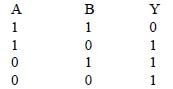
The following truth table corresponds to the logic gate [1991]

Detailed Solution: Question 8

This truth table is of identity, X = A + B, hence
OR gate.

31 Year NEET Previous Year Questions: Semiconductor Electronics - 4 - Question 9

To use a transistor as an amplifier [1991]

Detailed Solution: Question 9

To use a transistor as an amplifier the emitter
base junction is forward biased while the
collector base junction is reverse biased

31 Year NEET Previous Year Questions: Semiconductor Electronics - 4 - Question 10

Which one of the following is the weakest kindof bonding in solids [1992]

Detailed Solution: Question 10

Vander Waal’s bonding is the weakest
bonding in solids

31 Year NEET Previous Year Questions: Semiconductor Electronics - 4 - Question 11

For amplification by a triode, the signal to beamplified is given to [1992]

Detailed Solution: Question 11

The amplifying action of a triode is based on
the fact that a small change in grid voltage
causes a large change in plate current. The
AC input signal which is to be amplified is
superimposed on the grid potential.

31 Year NEET Previous Year Questions: Semiconductor Electronics - 4 - Question 12

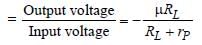
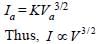
For an electronic valve, the plate current I andplate voltage V in the space charge limited regionare related as [1992]

Detailed Solution: Question 12

According to Child’s Law,

31 Year NEET Previous Year Questions: Semiconductor Electronics - 4 - Question 13

A piece of copper and other of germanium arecooled from the room temperature to 80 K, then    [1993]

Detailed Solution: Question 13

Copper is a conductor, so, its resistance
decreases on decreasing temperature as
thermal agitation decreases whereas
germanium is semiconductor, therefore, on
decreasing temperature resistance increases.

31 Year NEET Previous Year Questions: Semiconductor Electronics - 4 - Question 14

Diamond is very hard because [1993]

Detailed Solution: Question 14

Diamond is very hard due to large cohesive
energy.

31 Year NEET Previous Year Questions: Semiconductor Electronics - 4 - Question 15

The part of the transistor which is heavily dopedto produce large number of majority carriers is [1993]

Detailed Solution: Question 15

The function of emitter is to supply the
majority carriers. So, it is heavily doped

31 Year NEET Previous Year Questions: Semiconductor Electronics - 4 - Question 16

An oscillator is nothing but an amplifer with      [1994]

Detailed Solution: Question 16

A positive feed back from output to input in
an amplifier provides oscillations of constant
amplitude.

31 Year NEET Previous Year Questions: Semiconductor Electronics - 4 - Question 17

When a p-n junction diode is reverse biased theflow of current across the junction is mainly dueto [1994]

Detailed Solution: Question 17

When p-n junction is reverse biased, the flow
of current is due to drifting of minority charge
carriers across the junction.

31 Year NEET Previous Year Questions: Semiconductor Electronics - 4 - Question 18

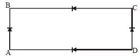
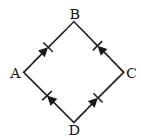
In Fig., the input is across the terminals A and C and the output is across B and D. Then the output is

Detailed Solution: Question 18

It is the circuit of full wave rectifier.

31 Year NEET Previous Year Questions: Semiconductor Electronics - 4 - Question 19

Which of the following gates corresponds tothe truth table given below?   [1994]

Detailed Solution: Question 19

This truth table is of the identity,    hence it is NAND gate.
Here, the output is high even if all inputs are low or one input is low.

31 Year NEET Previous Year Questions: Semiconductor Electronics - 4 - Question 20

In the diagram, the input is across the terminals A and C and the output is across B and D. Then the output is [1994, 02]

Detailed Solution: Question 20

The given circuit is a circuit of full wave
rectifier.

31 Year NEET Previous Year Questions: Semiconductor Electronics - 4 - Question 21

Which of the following, when added as animpurity, into the silicon, produces n-type semiconductor?   [1995]

Detailed Solution: Question 21

Phosphorous (P) is pentavalent and silicon
is tetravalent. Therefore, when silicon is
doped with pentavalent impurity, it forms a
n-type semiconductor.

31 Year NEET Previous Year Questions: Semiconductor Electronics - 4 - Question 22

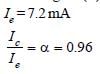
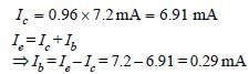
The current gain for a transistor working ascommon-base amplifier is 0.96. If the emittercurrent is 7.2 mA, then the base current is  [1996]

Detailed Solution: Question 22

Current gain (α) = 0.96

31 Year NEET Previous Year Questions: Semiconductor Electronics - 4 - Question 23

When an n–p–n transistor is used as an amplifierthen   [1996]

Detailed Solution: Question 23

In an n-p-n transistor, the charge carriers,
are free electrons in the transistor as well as
in external circuit; these electrons flow from
emitter to collector

31 Year NEET Previous Year Questions: Semiconductor Electronics - 4 - Question 24

When arsenic is added as an impurity to silicon,the resulting material is [1996]

Detailed Solution: Question 24

Arsenic contains 5 electrons in its outermost
shell. When Arsenic is mixed with silicon
there is one electron extra in silicon crystal.
Hence, such type of semi conductor is ntype
semi conductor

31 Year NEET Previous Year Questions: Semiconductor Electronics - 4 - Question 25

To obtain a p-type germanium semiconductor,it must be doped with   [1997]

Detailed Solution: Question 25

p-type germanium semiconductor is formed
when it is doped with a trivalent impurity
atom.

5 videos|87 docs|145 tests
Information about 31 Year NEET Previous Year Questions: Semiconductor Electronics - 4 Page
In this test you can find the Exam questions for 31 Year NEET Previous Year Questions: Semiconductor Electronics - 4 solved & explained in the simplest way possible. Besides giving Questions and answers for 31 Year NEET Previous Year Questions: Semiconductor Electronics - 4, EduRev gives you an ample number of Online tests for practice
5 videos|87 docs|145 tests
Download as PDF