Electronics and Communication Engineering (ECE) Exam  >  Electronics and Communication Engineering (ECE) Tests  >  Test: BJT As an Amplifier- 2 - Electronics and Communication Engineering (ECE) MCQ

Test: BJT As an Amplifier- 2 - Electronics and Communication Engineering (ECE) MCQ


Test Description

15 Questions MCQ Test - Test: BJT As an Amplifier- 2

Test: BJT As an Amplifier- 2 for Electronics and Communication Engineering (ECE) 2024 is part of Electronics and Communication Engineering (ECE) preparation. The Test: BJT As an Amplifier- 2 questions and answers have been prepared according to the Electronics and Communication Engineering (ECE) exam syllabus.The Test: BJT As an Amplifier- 2 MCQs are made for Electronics and Communication Engineering (ECE) 2024 Exam. Find important definitions, questions, notes, meanings, examples, exercises, MCQs and online tests for Test: BJT As an Amplifier- 2 below.
Solutions of Test: BJT As an Amplifier- 2 questions in English are available as part of our course for Electronics and Communication Engineering (ECE) & Test: BJT As an Amplifier- 2 solutions in Hindi for Electronics and Communication Engineering (ECE) course. Download more important topics, notes, lectures and mock test series for Electronics and Communication Engineering (ECE) Exam by signing up for free. Attempt Test: BJT As an Amplifier- 2 | 15 questions in 45 minutes | Mock test for Electronics and Communication Engineering (ECE) preparation | Free important questions MCQ to study for Electronics and Communication Engineering (ECE) Exam | Download free PDF with solutions
Test: BJT As an Amplifier- 2 - Question 1

The value of input impedance and voltage gain of the common base circuit shown below are respectively (Take VBE = 0.6 V)
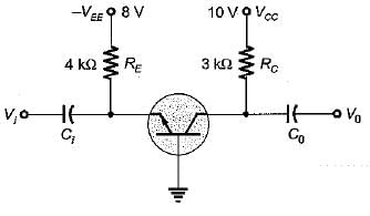
Detailed Solution for Test: BJT As an Amplifier- 2 - Question 1

Using AC equivalent circuit for the common base configuration, we can find that,

Now, 

∴ 
and AV = voltage gain

Test: BJT As an Amplifier- 2 - Question 2

The circuit shown in figure is biased such that VCE2 = 0 when VS = 0. Neglecting the base current of both transistors and forward bias across VBE  for both transistors to be 0.7, the value of RE would be equal to
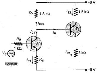
Detailed Solution for Test: BJT As an Amplifier- 2 - Question 2

Applying KVL, we have:

or, 
Also, 

∴ 
∴ 
When, Vi = 0,

or, 

1 Crore+ students have signed up on EduRev. Have you? Download the App
Test: BJT As an Amplifier- 2 - Question 3

A cascade stage is shown in figure below. If the transconductance of T1 and T2 are gm1 = ic1 / Vbe1 and gm2 = ic2 / Vbe2, the overall transconductance g= ic2 / Vbe1 is

Detailed Solution for Test: BJT As an Amplifier- 2 - Question 3


Here, 

Also, 


Hence, gm = gm1

Test: BJT As an Amplifier- 2 - Question 4

An emitter follower with β = 100 is biased at IC - 0.25 mA. The voltage source connected at its input has its internal resistance of 2 kΩ What is the value of RE such that it produces the output resistance of 110 Ω (Take VT = 25 mV)

Detailed Solution for Test: BJT As an Amplifier- 2 - Question 4


or, 
Now, 
Desired effective output resistance 

or, 
or,
or,
or,  

Test: BJT As an Amplifier- 2 - Question 5

Two stages of BJT amplifiers are cascaded by RC coupling. The voltage gain of the first stage is 20 and that of the second stage is 30. The overall gain of the coupled amplifier is

Detailed Solution for Test: BJT As an Amplifier- 2 - Question 5

The voltage gain of a multi-stage amplifier is equal to the product of the gains of the individual stages.

Test: BJT As an Amplifier- 2 - Question 6

The main characteristics of a Darlington amplifier are

Test: BJT As an Amplifier- 2 - Question 7

Which of the following parameters is used for distinguishing between a small signal and a large-signal amplifier?

Test: BJT As an Amplifier- 2 - Question 8

Consider the following statements:
1. The coupling capacitor mainly affect the lower cutoff frequency.
2. The phase reversal between output and input takes place only for voltage wave and not for current waves, in a transistor amplifier in CE mode.
3. The DC collector current in a transistor circuit is limited by the junction capacitance.
4. Negative DC feedback through RE is responsible for the stabilization of the operating point in a potential divider bias circuit.
​Of these statement:

Test: BJT As an Amplifier- 2 - Question 9

A transistor has hfe = 100, hte = 5.2 kΩ, and rbb, = 0. At room temperature V= 26 mV. The collector current |IC| will be

Detailed Solution for Test: BJT As an Amplifier- 2 - Question 9

hje= rbb' + rπ
Here, rbb' = 0 
Therefore, 
Now, 
∴ 
∴ 
= 0.5 mA

Test: BJT As an Amplifier- 2 - Question 10

A transistor is used in common emitter mode in an amplifier circuit. When a signal of 30 mV is added to the base emitter voltage, the base current changes by 30 μA and collector current by 3 mA. The load resistance is 5 kΩ. The value of transconductance and voltage gain is given by

Detailed Solution for Test: BJT As an Amplifier- 2 - Question 10


and 

Test: BJT As an Amplifier- 2 - Question 11

The transistor in the amplifier shown has the following parameters:
hfe = 100, hie = 2 kΩ, hre = 0, hoe = 0.05 m Mho.
'C’ is very large. The output impedance is
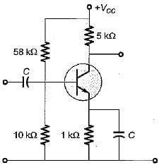
Detailed Solution for Test: BJT As an Amplifier- 2 - Question 11


or, 

Test: BJT As an Amplifier- 2 - Question 12

If RS is the source resistance, the output resistance of an emitter-follower using the simplified hybrid model would be

Detailed Solution for Test: BJT As an Amplifier- 2 - Question 12

If RS is the source resistance, the output resistance of an emitter-follower using the simplified hybrid model would be 

Test: BJT As an Amplifier- 2 - Question 13

In the CE amplifier with RL = 4000 Ω, given that The current gain |Ai| is

Detailed Solution for Test: BJT As an Amplifier- 2 - Question 13

Current gain,


or, 

Test: BJT As an Amplifier- 2 - Question 14

Assertion (A): On extending the hybrid model for two-port network to a transistor it is assumed that the signal excursion about the Q-point is small.
Reason (R): Small signal operation is that in which the AC input signal voltages and currents are in order of ±10% of Q-point voltage and currents.

Detailed Solution for Test: BJT As an Amplifier- 2 - Question 14

Both assertion and reason are correct statements.
The correct reason for assuming small signal excursion about the Q-point is to keep the transistor parameters constant over the signal excursion.

Test: BJT As an Amplifier- 2 - Question 15

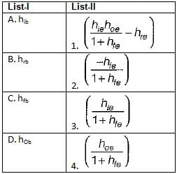
For a common-collector configuration of an n-p-n transistors, the hybrid parameters are given as:
hic = hie, hrc = - 1, hfc = - (1 + hfe) and hoc = hoe.
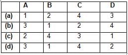
Match List-I (Hybrid parameters of CB configuration) with List-II (Values) and select the correct answer using the codes given below the lists:
Codes:
Information about Test: BJT As an Amplifier- 2 Page
In this test you can find the Exam questions for Test: BJT As an Amplifier- 2 solved & explained in the simplest way possible. Besides giving Questions and answers for Test: BJT As an Amplifier- 2, EduRev gives you an ample number of Online tests for practice

Top Courses for Electronics and Communication Engineering (ECE)

Download as PDF

Top Courses for Electronics and Communication Engineering (ECE)