GATE Exam  >  GATE Tests  >  Test: Basics and Power Semiconductor Devices - 1 - GATE MCQ

Test: Basics and Power Semiconductor Devices - 1 - GATE MCQ


Test Description

10 Questions MCQ Test - Test: Basics and Power Semiconductor Devices - 1

Test: Basics and Power Semiconductor Devices - 1 for GATE 2024 is part of GATE preparation. The Test: Basics and Power Semiconductor Devices - 1 questions and answers have been prepared according to the GATE exam syllabus.The Test: Basics and Power Semiconductor Devices - 1 MCQs are made for GATE 2024 Exam. Find important definitions, questions, notes, meanings, examples, exercises, MCQs and online tests for Test: Basics and Power Semiconductor Devices - 1 below.
Solutions of Test: Basics and Power Semiconductor Devices - 1 questions in English are available as part of our course for GATE & Test: Basics and Power Semiconductor Devices - 1 solutions in Hindi for GATE course. Download more important topics, notes, lectures and mock test series for GATE Exam by signing up for free. Attempt Test: Basics and Power Semiconductor Devices - 1 | 10 questions in 28 minutes | Mock test for GATE preparation | Free important questions MCQ to study for GATE Exam | Download free PDF with solutions
Test: Basics and Power Semiconductor Devices - 1 - Question 1

Figure shows four electronic switches (i), (ii), (iii) and (iv). Which of the switches can block voltages of either polarity (applied between terminals a and b) when the active device is in the OFF state?

a a a a
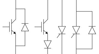
b b b b

Test: Basics and Power Semiconductor Devices - 1 - Question 2

The MOSFET switch in its on-state may be considered equivalent to

Detailed Solution for Test: Basics and Power Semiconductor Devices - 1 - Question 2
MOSFET in its on state gives a variable resistance depending upon the magnitude of gate voltage. Therefore, it can be treated as a resistor. Hence, the correct option is (a).
1 Crore+ students have signed up on EduRev. Have you? Download the App
Test: Basics and Power Semiconductor Devices - 1 - Question 3

The typical ratio of latching current to holding current in a 20 A thyristor is

Detailed Solution for Test: Basics and Power Semiconductor Devices - 1 - Question 3
Typical ratio of latching current to holding current lies in the range of 2.5 to 3. Therefore, only 2.0 is the nearest option. Hence, the correct option is (b).
Test: Basics and Power Semiconductor Devices - 1 - Question 4

Circuit turn-off time of an SCR is defined as the time

Detailed Solution for Test: Basics and Power Semiconductor Devices - 1 - Question 4
Hence, the correct option is (c).
Test: Basics and Power Semiconductor Devices - 1 - Question 5

Figure shows a composite switch consisting of a power transistor (BJT) in series with a diode. Assume that the transistor switch and the diode are ideal. The I–V characteristic of the composite switch is

Detailed Solution for Test: Basics and Power Semiconductor Devices - 1 - Question 5
Hence, the correct option is (c).
Test: Basics and Power Semiconductor Devices - 1 - Question 6

An SCR is considered to be a semi controlled device because

Detailed Solution for Test: Basics and Power Semiconductor Devices - 1 - Question 6
Application of negative gate pulse to a conducting thyristor cannot turn-off the device. Therefore, only the turn-on of the SCR can be controlled using a gate pulse. Hence, it is called a semi controlled switch. Hence, the correct option is (c).
Test: Basics and Power Semiconductor Devices - 1 - Question 7

The conduction loss versus device current characteristic of a power MOSFET is best approximated by

Detailed Solution for Test: Basics and Power Semiconductor Devices - 1 - Question 7
The conduction loss in a MOSFET is due to the variable resistance path during the on-state.

∴ Ploss = I2ds (RChannel + Rdevice)

= I2ds RON*

∴ Conduction loss versus device current graph will be a parabola. Hence, the correct option is (a).

Test: Basics and Power Semiconductor Devices - 1 - Question 8

A bipolar junction transistor (BJT) is used as a power control switch by biasing it in cut-off region (OFF state) or in the saturation region (ON state). In the ON state, for the BJT,

Detailed Solution for Test: Basics and Power Semiconductor Devices - 1 - Question 8

Cut off region: Both base–emitter and base–collector junctions are reverse biased. Saturation region: Both base–emitter and base– collector junctions are forward biased. Hence, the correct option is (d).

Test: Basics and Power Semiconductor Devices - 1 - Question 9

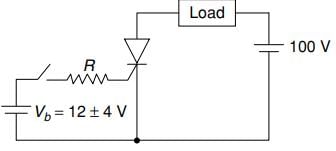
The triggering circuit of a thyristor is shown in figure. The thyristor requires a gate current of 10 mA, for guaranteed turn-on. The value of R required for the thyristor to turn on reliably under all conditions of Vb variation is
Detailed Solution for Test: Basics and Power Semiconductor Devices - 1 - Question 9
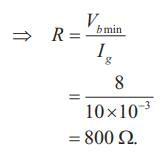
Thyristor requires a gate current of 10 mA to turn on. Thyristor will turn on under any voltage conditions only when minimum gate voltage can produce the necessary gate current.

∴ = Vbmin =12 − = 4 = 8 V.

Applying KVL in the gate circuit, we get,Vbmin = I g R.

Hence, the correct option is (d).

Test: Basics and Power Semiconductor Devices - 1 - Question 10

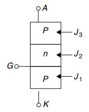
Figure shows a thyristor with the standard terminations of anode (A), cathode (K), gate (G) and the different junctions named J1 , J2 and J3 . When the thyristor is turned on and conducting
Detailed Solution for Test: Basics and Power Semiconductor Devices - 1 - Question 10

When an SCR is in the on-state or in conduction state, all the junctions are forward biased. Hence, the correct option is (d).

Information about Test: Basics and Power Semiconductor Devices - 1 Page
In this test you can find the Exam questions for Test: Basics and Power Semiconductor Devices - 1 solved & explained in the simplest way possible. Besides giving Questions and answers for Test: Basics and Power Semiconductor Devices - 1, EduRev gives you an ample number of Online tests for practice
Download as PDF