Electronics and Communication Engineering (ECE) Exam  >  Electronics and Communication Engineering (ECE) Tests  >  Test: Carrier Transport - 2 - Electronics and Communication Engineering (ECE) MCQ

Test: Carrier Transport - 2 - Electronics and Communication Engineering (ECE) MCQ


Test Description

10 Questions MCQ Test - Test: Carrier Transport - 2

Test: Carrier Transport - 2 for Electronics and Communication Engineering (ECE) 2024 is part of Electronics and Communication Engineering (ECE) preparation. The Test: Carrier Transport - 2 questions and answers have been prepared according to the Electronics and Communication Engineering (ECE) exam syllabus.The Test: Carrier Transport - 2 MCQs are made for Electronics and Communication Engineering (ECE) 2024 Exam. Find important definitions, questions, notes, meanings, examples, exercises, MCQs and online tests for Test: Carrier Transport - 2 below.
Solutions of Test: Carrier Transport - 2 questions in English are available as part of our course for Electronics and Communication Engineering (ECE) & Test: Carrier Transport - 2 solutions in Hindi for Electronics and Communication Engineering (ECE) course. Download more important topics, notes, lectures and mock test series for Electronics and Communication Engineering (ECE) Exam by signing up for free. Attempt Test: Carrier Transport - 2 | 10 questions in 30 minutes | Mock test for Electronics and Communication Engineering (ECE) preparation | Free important questions MCQ to study for Electronics and Communication Engineering (ECE) Exam | Download free PDF with solutions
Test: Carrier Transport - 2 - Question 1

A Hall-effect element is used for the measurement of magnetic field of 0.8 Wb/m2. The thickness of the element is 2.5 mm and is of bismuth material. If the current passed through the element is 4A, then the Hall emf developed will be: (Hall coefficient is 5 × 10⁻⁷)

Detailed Solution for Test: Carrier Transport - 2 - Question 1

Concept: 

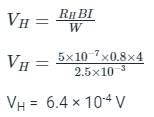
The hall voltage VA is given by:

ρc: Charge density

RH: Hall coefficient

W is the side across which the magnetic field is applied.

Calculation:

W = Thickness = 2.5 mm, I = 4A, RH = 5 x 10⁻⁷, B = 0.8 Wb/m2  

Test: Carrier Transport - 2 - Question 2

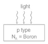
A bar of silicon is doped with a boron concentration of 1016 cm-3 and assumed to be fully ionized. It is exposed to light such that electron-hole pairs are generated throughout the volume of the bar at the rate of 1020 cm-3s-1. If the recombination lifetime is 100 μs, the intrinsic carrier concentration of silicon is 1010 cm-3 and assuming 100% ionization of boron, then the approximate product of steady-state electron and hole concentrations due to this light exposure is

Detailed Solution for Test: Carrier Transport - 2 - Question 2

Concept:

The number of minority carriers generated because of light is given by the generation rate as:

Analysis:

NA = 1016 / cm3

G = 1020 / cm3 – sec

τ = 100 μsec

ni = 1010 / cm3

before shining light:

Hole concertration (p) ≃ NA = 1016 / cm3

Electron concentration (n)

After illumination of light minority carrier will be generated.

So after light illumination hole conc. (p’) = p + Δp

p’ = 1016 + 1020 × 10-6 × 100

= 2 × 10¹⁶ / cm3

After illumination e- conc. (n’) = n + Δn

= 104 + 1020 × 10-6 × 100

≃ 1016 / cm3

Product of e- and hole concertration = n’ × p’

= 2 × 1032 / cm-6

1 Crore+ students have signed up on EduRev. Have you? Download the App
Test: Carrier Transport - 2 - Question 3

A semiconductor bar having a length of 4 cm is subjected to a voltage of 8 Volts. If the average drift velocity is 104 cm/s, then electron mobility would be:

Detailed Solution for Test: Carrier Transport - 2 - Question 3

Concept:

Mobility of charge carriers (μ) defines how fast the charge carriers or travel from one place to another.

It is drift velocity (saturation velocity) per unit electric field. i.e

vd = Drift velocity (Saturation velocity)

E = Electric field given by:

Calculation:

L = 4 cm

V = 8 Volts

vd = 104 cm/s

from Equation (2):

From equation (1):

Important Point

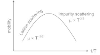
  • Mobility increases due to lattice scattering and decreases due to impurity scattering
  • At low temperatures only impurity scattering is dominant and at high temperatures lattice scattering is dominant
  • Mobility first increases with temperature and then subsequently decreases

Note: The term impurity in an intrinsic semiconductor:

Impurity scattering is caused by crystal defects such as ionized impurities.

At lower temperatures, carriers move more slowly, so there is more time for them to interact with charged impurities.

As a result, as the temperature decreases, impurity scattering increases, and mobility decreases.

The effect is just the opposite of the effect of lattice scattering.

Test: Carrier Transport - 2 - Question 4

If σ is the conductivity, What is the relation between the electric field E and the current density J in a conducting medium?

Detailed Solution for Test: Carrier Transport - 2 - Question 4

Concept:

Ohms’ law: At constant temperature, the current through a resistance is directly proportional to the potential difference across the resistance.

V = R I

Where V is the potential difference, R is resistance and I is current flowing

Current density (J): The electric current per unit area is called current density.

Conductivity (σ): The property of a conductor due to which the current flows through it is called the conductivity of that conductor.

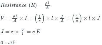
Where ρ is resistivity = 1/σ, l is the length and A is the area of the conductor

Electric field (E) = potential difference (V)/length (l)

Analysis:

As, V = R I 

Test: Carrier Transport - 2 - Question 5

Drift velocity in metal is

Detailed Solution for Test: Carrier Transport - 2 - Question 5

Concept:

The drift velocity is directly proportional to the electric field, i.e.

Vd ∝ E

Vd = μE

The proportionality constant 'μ' defined as:

Observation: 

  • Drift velocity is proportional to the mobility of the electron, i.e. more the mobility, the more will be the drift velocity.
  • Drift velocity is directly proportional to the electric field applied.
  • Drift velocity is inversely proportional to the mass of the electron.

Notes:

  • Mobility defines how quickly can an electron move in metal or semiconductor under the influence of the electric field.
  • When an electric field is applied, the electrons and holes are accelerated by it.
  • The electron moving with a finite average velocity is called drift velocity.
Test: Carrier Transport - 2 - Question 6

The Hall Effect may be used to 

1. Determine whether the semiconductor is p-type or n - type.

2. Determine the carrier concentration.

3. Calculate the mobilty.

Which of the above statements are correct?

Detailed Solution for Test: Carrier Transport - 2 - Question 6

Hall Effect:

It states that if a specimen (metal or semiconductor) carrying a current (I) is placed in a transverse magnetic field (B), an electric field is induced in the direction perpendicular to both I and B.

Hall Voltage is given by:


The hall coefficient is given as:

Where,

ρ = charge density = σ / μ 

n = charge concentration

σ = conductivity

μ = mobility constant

Hence Hall coefficient becomes

  • The Hall effect provides information on the sign, concentration, and mobility of charge carriers in the normal state.
  • A positive sign for the Hall coefficient indicates that the majority carriers are holes and semiconductor is P-type.
  • A negative sign for the Hall coefficient indicates that the majority carriers are electrons and semiconductor is N-type.

Applications of Hall-effect: 

Hall effect can be used to find:

1. Carrier concentration

2. Type of semiconductor

3. Conductivity

4. Mobility

It cannot be used to find a magnetic field.

Common Confusion Point:

Looking at the formula one can think that the magnetic field can be calculated but in HALL Experiment, perpendicular MAGNETIC field and electric field are applied on the material and other parameters are measured.

Test: Carrier Transport - 2 - Question 7

Select the correct statement about a semiconductor

Detailed Solution for Test: Carrier Transport - 2 - Question 7

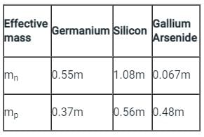
Where m: mass

Observations:

1) The effective mass of the hole is greater than that of the electron.

2) The relaxation times are often of the same order of magnitude for electrons and holes and therefore, they do not make too much difference.

As the effective mass is less for electron it moves faster than that of the hole.
Important Point
Drift velocity


vd  = μ × E

μ: Mobility of charge carrier

Drift velocities of Hole and Electron

Vn = μn × E

Vp = μp × E

*Answer can only contain numeric values
Test: Carrier Transport - 2 - Question 8

At T = 300 K, the hole mobility of a semiconductor μp = 500 cm2/V-s and kT/q = 26mV. The hole diffusion constant Dp in cm2/s is _______


Detailed Solution for Test: Carrier Transport - 2 - Question 8

Concept:

The mobility of a carrier is related to the diffusion coefficient through Einstein’s relation as:

Dp = Hole diffusion density

μp = Mobility of holes

Calculation:

With μp = 500 cm2 / V-S and KT/q = 26mV, we can write:

Dp/500 = 26m 

Dp = 500 × 26 m

Dp = 13000 m cm2 / s

Dp = 13 cm2 / s

Test: Carrier Transport - 2 - Question 9

Charge carriers can move in semiconductor via:

Detailed Solution for Test: Carrier Transport - 2 - Question 9

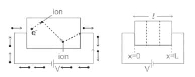
Charge carriers can move in a semiconductor because of two phenomena:

Drift Mechanism:

  • Under the action of an electric field, the charge carriers in the semiconductor material stop moving randomly and start drifting towards or away the applied electric field depends upon their nature.
  • This drift of charge carriers produces drift current.
  • For drift current external electric field is essential.
  • It depends on carrier concentration and the external electric field.

Diffusion Mechanism:

  • In a semiconductor, there may arise a situation where the concentration of charge carriers within the crystal becomes different and hence producing concentration gradient, due to which charge carriers cross the surface to maintain equilibrium and constitute a current which is known as diffusion current.
  • For diffusion, the current external field is not required. Any external energy may stimulate this process.
  • It depends upon the rate of charge of carrier concentration per unit length.
Test: Carrier Transport - 2 - Question 10

Pure Metals generally have

Detailed Solution for Test: Carrier Transport - 2 - Question 10

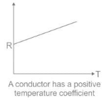
In Metals:

  • The conductivity of pure metals is very high due to a large number of free electrons. 
  • As the temperature increases, the carrier concentration remains almost the same, but there is a decrease in mobility due to lattice scattering. 
  • Hence resistivity increases, which implies the temperature coefficient of resistivity for metals is positive. 

Important Point

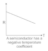
In Semiconductors:

  • As the temperature increases, the carrier concentration increases significantly, this is because extra electrons are excited from the valence band to the conduction band, due to which the number of free electrons increases.
  • So that conductivity increases & resistivity decreases, which implies the temperature coefficient of resistivity is negative intrinsic semiconductors
  • The dominant factor is the number of free electrons and hence specific resistance of semiconductor decreases with increasing temperature
  • The difference in the variation of resistance with temperature in a metal and a semiconductor arises essentially due to the difference in the variation of the number of charge carriers with temperature.

Information about Test: Carrier Transport - 2 Page
In this test you can find the Exam questions for Test: Carrier Transport - 2 solved & explained in the simplest way possible. Besides giving Questions and answers for Test: Carrier Transport - 2, EduRev gives you an ample number of Online tests for practice

Top Courses for Electronics and Communication Engineering (ECE)

Download as PDF

Top Courses for Electronics and Communication Engineering (ECE)