Electronics and Communication Engineering (ECE) Exam  >  Electronics and Communication Engineering (ECE) Tests  >  Test: CMOS Implementation - Electronics and Communication Engineering (ECE) MCQ

Test: CMOS Implementation - Electronics and Communication Engineering (ECE) MCQ


Test Description

10 Questions MCQ Test - Test: CMOS Implementation

Test: CMOS Implementation for Electronics and Communication Engineering (ECE) 2024 is part of Electronics and Communication Engineering (ECE) preparation. The Test: CMOS Implementation questions and answers have been prepared according to the Electronics and Communication Engineering (ECE) exam syllabus.The Test: CMOS Implementation MCQs are made for Electronics and Communication Engineering (ECE) 2024 Exam. Find important definitions, questions, notes, meanings, examples, exercises, MCQs and online tests for Test: CMOS Implementation below.
Solutions of Test: CMOS Implementation questions in English are available as part of our course for Electronics and Communication Engineering (ECE) & Test: CMOS Implementation solutions in Hindi for Electronics and Communication Engineering (ECE) course. Download more important topics, notes, lectures and mock test series for Electronics and Communication Engineering (ECE) Exam by signing up for free. Attempt Test: CMOS Implementation | 10 questions in 30 minutes | Mock test for Electronics and Communication Engineering (ECE) preparation | Free important questions MCQ to study for Electronics and Communication Engineering (ECE) Exam | Download free PDF with solutions
Test: CMOS Implementation - Question 1

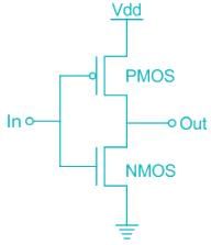
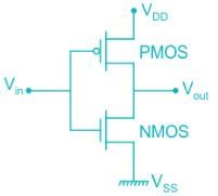
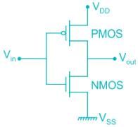
The above circuit acts as:

Detailed Solution for Test: CMOS Implementation - Question 1

Inverter
This is equal to NOT gate in the digital circuitry.
The output of this is a compliment of the input.

This can be built from the transistors like BJT, MOSFET, etc…
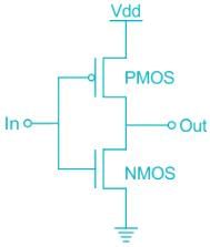
The CMOS inverter consists of the NMOS and the PMOS field-effect transistors connected in one below the other.

When In = Low
PMOS will be shorted and output will be High.
When In = High
NMOS will be shorted and output will be Low.
Hence it acts as an inverter.

Test: CMOS Implementation - Question 2

Which one of the following statements is not correct for CMOS technology in comparison with bipolar technology?

Detailed Solution for Test: CMOS Implementation - Question 2

Comparison between CMOS and BJT technology:

  • CMOS technology allows the power dissipation to be low and gives more power output, whereas bipolar takes lots of power to run the system and the circuitry requires lots of power to get activated.
  • CMOS technology provides high input impedance which is a low drive current that allows more current to be flown in the circuit and keeps the circuit in a good position, whereas it provides a high drive current means more input impedance.
  • CMOS technology provides scalable threshold voltage more in comparison to Bipolar technology which provides low threshold voltage.
  • CMOS technology provides a high noise margin and packing density whereas Bipolory technology allows having a low noise margin to reduce the high values and give a low packing density of the components.
1 Crore+ students have signed up on EduRev. Have you? Download the App
Test: CMOS Implementation - Question 3

A digital CMOS IC operating at 15 MHz clock frequency consumes 130 mW, the same IC operating at 10 MHz clock frequency consumes 100 mW power. The static power consumption of the IC is?

Detailed Solution for Test: CMOS Implementation - Question 3

Static power is proportional to the static current, i.e. the current that flows regardless of gate switching.
Dynamic Power is related to the current that flows when switching takes place and is given by for CMOS as:
P = fCV2cc
Or P = Kf (where K = Vcc2C)
Power consumed by CMOS = Pstatic + Pdynamic
Calculation:-
For f1 = 15 MHz, Pconsumed = 130 mW → P1
f2 = 10 MHz, Pconsumed = 100 mW → P2
p1 = pstatic + pdynamic
130 = pstatic + K f1
130 = pstatic + K (15 MHz)      ---(1)
100 = pstatic + K (10 MHz)      ---(2)
30 × 10-3 = 5 × 10⁶ K
Putting the value of K in equation (1), we get
Pstatic = 
= 40 mW

Test: CMOS Implementation - Question 4

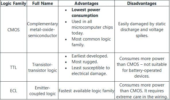
The full forms of the abbreviations TTL and CMOS in reference to logic families are

Detailed Solution for Test: CMOS Implementation - Question 4

TTL stands for Transistor-Transistor Logic and CMOS stands for Complimentary Metal Oxide Semiconductor.

Test: CMOS Implementation - Question 5

Which circuit takes the less chip area in large scale integration?

Detailed Solution for Test: CMOS Implementation - Question 5

In large scale integration (LSI), CMOS (complementary Metal-oxide Semiconductor) circuit takes the less Chip area during fabrication. This is because the CMOS circuit is a combination of NMOS and PMOS and it is fabricated as a twin tub process where the required Chip area is less.
During the process of bipolar logic families (such as RTL, DTCL, DTL, HTL, TTL, and ECL) fabrication, required large chip area as these circuits consist of NPN and PNP transistor, diodes, resistors, etc.
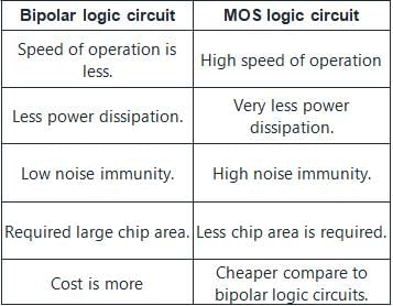
Important Comparison between bipolar logic circuits and MOS logic circuits:

Test: CMOS Implementation - Question 6

The typical quiescent power dissipation of low-power CMOS units is

Detailed Solution for Test: CMOS Implementation - Question 6

Complementary Metal-oxide-semiconductor (CMOS) uses complementary & symmetrical pair of P-type & n-type MOSFETS.

  • The two important characteristics of CMOS devices are high noise immunity and low power dissipation.
  • CMOS devices dissipate less power than NMOS devices because the CMOS dissipates power only when switching (“dynamic power), whereas N channel MOSFET dissipates power whenever the transistor is on because there is a current path from Vdd to Vss.
  • In a CMOS, only one MOSFET is switched on at a time. Thus, there is no path from voltage source to ground so that a current can flow. Current flows in a MOSFET only during switching.
  • Thus, compared to N-channel MOSFET has the advantage of lower drain current from the power supply, thereby causing less power dissipation.
  • The typical quiescent power dissipation of low-power CMOS units is 2 nW.
Test: CMOS Implementation - Question 7

The main advantage of CMOS is its

Detailed Solution for Test: CMOS Implementation - Question 7

The most important parameters for evaluating and comparing logic families are:

  • Power dissipation
  • Propagation delay
  • Noise margin
  • Fan-out (loading)

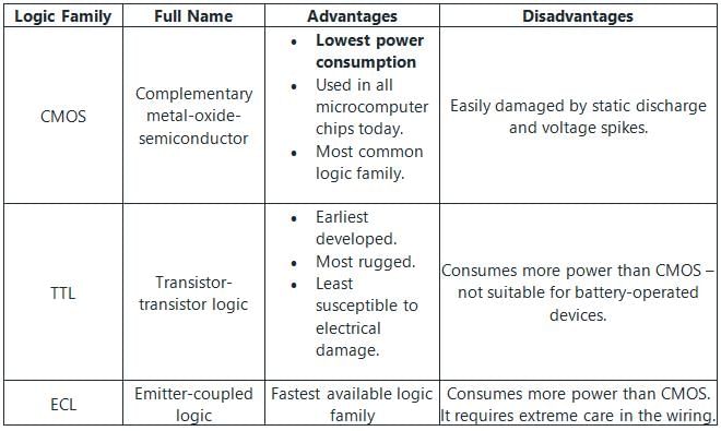
General comparison of three commonly available logic families is explained in the following table:

Test: CMOS Implementation - Question 8

As compared to TTL, CMOS logic has

Detailed Solution for Test: CMOS Implementation - Question 8

Option(1)- Schottky transistors are  preferred for TTL logic systems. These transistors portray the Schottky effect and thus have higher switching speed in comparison to CMOS logic family.So option 1 is false.
Option(2)- TTL dissipates a lot of power where as CMOS uses almost no power in the static state (that is, when inputs are not changing). So option 2  is false.
Option(3)- TTL  requires more space and isolation in comparison to CMOS logic family. The required silicon area for implementing  CMOS  is very small. So option 3  is true.
Important Point-
1.
 Characteristics of CMOS Logic Families-

  • Has the highest fan-out, when compared with TTL and ECL
  • Works well over a wide range of temperature
  • Noise immunity is better than TTL and ECL

2. Characteristics of TTL Logic Families-

  • Fastest saturation, when compared to other logic families
  • Low output impedance for all states
  • TTL dissipates a lot of power, thus not making it suitable for battery-powered devices.
Test: CMOS Implementation - Question 9

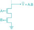
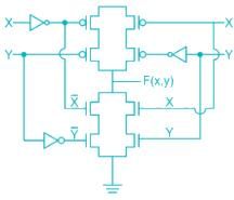
The logic function f(X,Y) realized by the given circuit is

Detailed Solution for Test: CMOS Implementation - Question 9

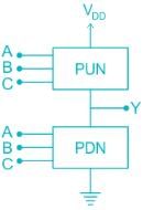
CMOS logic circuit is an extension of a CMOS inverter. It consists of two network transistors, a pull-down network (PDN) constructed of an n-MOS and Pull-up Network (PUN) constructed of P-MOS.

PDN: Since nMOS conducts when the signal gate is high, PDN is activated when the inputs are high.
PUN: It comprises PMOS and conducts when the input signal gate is low.
The PDN and PUN are connected in parallel to form OR logic function and they are connected in series to form AND logic as shown:


Application:

Test: CMOS Implementation - Question 10

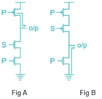
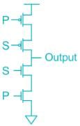
Output of the circuit shown below when S = 1 and S = 0 will be _____.
Detailed Solution for Test: CMOS Implementation - Question 10

Complementary Metal-oxide-semiconductor (CMOS) uses complementary & symmetrical pair of P-type & n-type MOSFETS.

  • The two important characteristics of CMOS devices are high noise immunity and low power dissipation.
  • In CMOS, during static operation at a time, only one MOS is ON i.e. either PMOS or NMOS. So there is no direct path from the power supply to the ground. Hence, Power dissipation in CMOS is low in static operation but it has high power dissipation in dynamic operation.

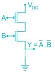
As the given figure is of CMOS with two inputs.

The upper part is PMOS which is switched on when 0 is applied and NMOS is switched on when 1 is applied.

1. When S = 0 is applied, the PMOS connected to S (upper one) will be shorted and P at PMOS will appear across the output in complemented form as shown in fig(A).
So Output = P̅
2. Now when S = 1 is applied, the NMOS connected to S (lower one) will be shorted, and due to which ground will appear across the output and the circuit will go in a high impedance state as shown in fig(B).
Hence option (2) is the correct answer.

Information about Test: CMOS Implementation Page
In this test you can find the Exam questions for Test: CMOS Implementation solved & explained in the simplest way possible. Besides giving Questions and answers for Test: CMOS Implementation, EduRev gives you an ample number of Online tests for practice

Top Courses for Electronics and Communication Engineering (ECE)

Download as PDF

Top Courses for Electronics and Communication Engineering (ECE)