Test: Analog & Digital Electronics - 1 - Electrical Engineering (EE) MCQ
10 Questions MCQ Test - Test: Analog & Digital Electronics - 1
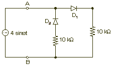
A voltage V = 4 sin ωt is applied to the terminals A and B of the circuit shown in figure. The diodes are assumed to be ideal. The impedance offered by the circuit across the terminals A and B in kilo-ohms is

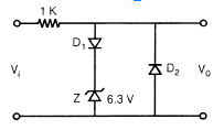
Consider the following limiter circuit an input voltage V| = 10.5 sinlOOnt is applied. Assume that the diode drop is 0.7 V in forward bias. The zener breakdown voltage is 6.3 V.

The maximum and minimum values of the output voltage respectively are
In the saturation region of a BJT (Bipolar Junction Transistor)
Given below is the Ic Vs VCE characteristic of two npn transistor P and Q having current gains β1 and β2 respectively.
Hard lines: Characteristics of P Dashed lines: Characteristics of Q
Which of the following is true?
The thermal run-away in a CE-transistor amplifier can be prevented by biasing in such a wav that.
IDSS = 8 mA Vp = -5 V, Assume Gate current » 0 all the capacitance used are of very large value. The voltage gain Av, is
If the differential voltage gain and the common mode voltage gain of a differential amplifier are 50-dB and 2-dB resDectivelv. then its common mode rejection ratio is
Which of the following instruments has a uniform scale?
Consider the following op-amp circuit with multiple stages:
Shown below is a positive feedback arrangement to generate sinusoidal oscillation


