


All questions of Digital Logic for Computer Science Engineering (CSE) Exam
Which of these sets of logic gates are known as universal gates?- a)XOR, NAND, OR
- b)OR, NOT, XOR
- c)NOR, NAND, XNOR
- d)NOR, NAND
Correct answer is option 'D'. Can you explain this answer?
Which of these sets of logic gates are known as universal gates?
a)
XOR, NAND, OR
b)
OR, NOT, XOR
c)
NOR, NAND, XNOR
d)
NOR, NAND
|
|
Sudhir Patel answered |
NAND or NOR gates are used to design all other logic gates, so; they are termed universal gates.

Which of the following is equal to 1?- a)20 + 30 + 40
- b)20 × 30 × 40
- c)(30 – 20) × 40
- d)(30 – 20) × (30 + 20)
Correct answer is option 'B'. Can you explain this answer?
Which of the following is equal to 1?
a)
20 + 30 + 40
b)
20 × 30 × 40
c)
(30 – 20) × 40
d)
(30 – 20) × (30 + 20)
|
|
Devanshi Desai answered |
None of the options are equal to 1.
A classification of integrated circuits with complexities of 30 to 300 equivalent gates on a single chip is known as?- a)VLSI
- b)SSI
- c)LSI
- d)MSI
Correct answer is option 'D'. Can you explain this answer?
A classification of integrated circuits with complexities of 30 to 300 equivalent gates on a single chip is known as?
a)
VLSI
b)
SSI
c)
LSI
d)
MSI
|
|
Arpita Mehta answered |
MSI (Medium-Scale Integration) Integrated Circuits
MSI integrated circuits are a classification of ICs that have complexities ranging from 30 to 300 equivalent gates on a single chip.
Characteristics of MSI Integrated Circuits:
- MSI ICs are more complex than SSI (Small-Scale Integration) ICs but less complex than LSI (Large-Scale Integration) and VLSI (Very Large-Scale Integration) ICs.
- They typically contain multiple logic gates, flip-flops, and other components on a single chip.
- MSI ICs are used in a variety of applications such as arithmetic units, multiplexers, encoders, and decoders.
Advantages of MSI Integrated Circuits:
- They offer a higher level of integration compared to SSI ICs, which leads to smaller size, lower power consumption, and improved performance.
- MSI ICs are more cost-effective than LSI and VLSI ICs for applications that require moderate complexity.
Applications of MSI Integrated Circuits:
- MSI ICs are commonly used in consumer electronics, industrial automation, telecommunications, and other fields where moderate complexity and cost efficiency are important factors.
- They play a crucial role in the design of various digital systems and devices.
In conclusion, MSI integrated circuits fill the gap between SSI and LSI/VLSI ICs by providing a moderate level of complexity and integration suitable for a wide range of applications.
How many bits are needed to store one BCD digit?- a)2 bits
- b)4 bits
- c)3 bits
- d)1 bit
Correct answer is option 'B'. Can you explain this answer?
How many bits are needed to store one BCD digit?
a)
2 bits
b)
4 bits
c)
3 bits
d)
1 bit
|
|
Arindam Goyal answered |
BCD stands for Binary Coded Decimal. It is a form of representing decimal numbers using a binary code. In BCD, each decimal digit is represented by a 4-bit binary code. Let's break down the answer and explain why it is option 'B' - 4 bits.
Binary Coded Decimal (BCD)
BCD is a way of representing decimal digits using a binary code. In BCD, each decimal digit is represented by a 4-bit binary code. This means that 4 binary bits are required to represent a single BCD digit.
Binary Digits
In binary representation, each digit can take on one of two values, 0 or 1.
Decimal Digits
In decimal representation, each digit can take on one of ten values, from 0 to 9.
BCD Representation
To represent decimal digits using BCD, each decimal digit is divided into its binary equivalent. For example, the decimal digit 0 is represented as 0000 in BCD, 1 as 0001, 2 as 0010, and so on up to 9 as 1001.
Number of Bits for a BCD Digit
Since each decimal digit is represented by a 4-bit binary code in BCD, we can conclude that 4 bits are required to store one BCD digit.
Examples
Let's consider some examples to further illustrate this:
- The BCD representation of the decimal digit 3 is 0011, which requires 4 bits.
- The BCD representation of the decimal digit 7 is 0111, which also requires 4 bits.
- The BCD representation of the decimal digit 9 is 1001, again requiring 4 bits.
Conclusion
In conclusion, 4 bits are required to store one BCD digit. This is because each decimal digit is represented by a 4-bit binary code in BCD. Therefore, the correct answer is option 'B' - 4 bits.
In an 8 -bit Johnson counter sequence, how many states orbit patterns are possible?- a)240
- b)228
- c)232
- d)220
Correct answer is option 'A'. Can you explain this answer?
In an 8 -bit Johnson counter sequence, how many states orbit patterns are possible?
a)
240
b)
228
c)
232
d)
220
|
|
Niti Basu answered |
Explanation:
To calculate the number of states or bit patterns in an 8-bit Johnson counter sequence, we need to understand the concept of a Johnson counter and its sequence.
A Johnson counter is a modified version of a ring counter. It is a sequential circuit that cycles through a fixed sequence of states. In an 8-bit Johnson counter, there are 8 flip-flops connected in a ring, forming a circular shift register.
Johnson Counter Sequence:
The sequence of states in a Johnson counter follows a specific pattern. It starts with all bits set to 0 and then cycles through a sequence of 2^n - 1 states, where n is the number of bits in the counter.
In an 8-bit Johnson counter, the sequence will have 2^8 - 1 = 255 states. However, we need to exclude the initial state (all bits set to 0) from the count.
Therefore, the number of states in the Johnson counter sequence is 255 - 1 = 254.
Orbit Patterns:
An orbit pattern is a subset of the Johnson counter sequence that represents a complete cycle or loop. It starts and ends at the same state.
To calculate the number of orbit patterns, we need to find the number of states in each orbit pattern. In an 8-bit Johnson counter, each orbit pattern will have 8 states, as it takes 8 clock cycles for the counter to return to its initial state.
The total number of possible orbit patterns can be calculated by dividing the total number of states in the Johnson counter sequence by the number of states in each orbit pattern.
Total number of states = 254
Number of states in each orbit pattern = 8
Number of orbit patterns = Total number of states / Number of states in each orbit pattern
= 254 / 8
= 31.75
Since the number of orbit patterns cannot be a fraction, we round it down to the nearest whole number.
Therefore, the number of orbit patterns in an 8-bit Johnson counter sequence is 31.
Conclusion:
The correct answer is option A) 240.
The planet Uranus is approximately 2,896,819,200,000 metres away from the Sun. What is this distance in standard form?- a)2.8968192 × 10¹² m
- b)2.8968192 × 10¹³ m
- c)28968192 × 1013 m
- d)289.68192 × 10¹² m
Correct answer is option 'A'. Can you explain this answer?
The planet Uranus is approximately 2,896,819,200,000 metres away from the Sun. What is this distance in standard form?
a)
2.8968192 × 10¹² m
b)
2.8968192 × 10¹³ m
c)
28968192 × 1013 m
d)
289.68192 × 10¹² m
|
|
Rashi Singh answered |
X 10^12 metres
b) 2.8968192 x 10^11 metres
c) 2.8968192 x 10^13 metres
d) 2.8968192 x 10^14 metres
Answer: c) 2.8968192 x 10^13 metres
b) 2.8968192 x 10^11 metres
c) 2.8968192 x 10^13 metres
d) 2.8968192 x 10^14 metres
Answer: c) 2.8968192 x 10^13 metres
Which coding scheme is used in computer to represent data internally?- a)Decimal
- b)Integral
- c)Binary
- d)None of the above
Correct answer is option 'C'. Can you explain this answer?
Which coding scheme is used in computer to represent data internally?
a)
Decimal
b)
Integral
c)
Binary
d)
None of the above

|
Cstoppers Instructors answered |
Key Points
- Internally the computer coding scheme represents data in Binary form
- The computer is an electronic device, which accepts data, processes it and outputs the results in the form of reports.
- The original objective of computers was to make fast calculations, but modern computers besides performing fast calculations can store large volumes of data, process and retrieve data as and when desired.
- Hence computers are also known as data processors.
- The computer is a system. A system is a group of integrated parts to achieve a common objective.
- The computer is made up of integrated parts (input, control, ALU, storage, and output unit).
- All the parts work together to process data.
- The computer accepts input and outputs data in an alphanumeric form. Internally it converts the input data to meaning binary digits, performs the instructed operations on the binary data, and transforms the data from binary digit form to understandable alphanumeric form.
At which frequency the digital data can be applied to a gate?- a)Run-time frequency
- b)Propagation Frequency
- c)Operating frequency
- d)AC frequency
Correct answer is option 'C'. Can you explain this answer?
At which frequency the digital data can be applied to a gate?
a)
Run-time frequency
b)
Propagation Frequency
c)
Operating frequency
d)
AC frequency
|
|
Sudhir Patel answered |
The operating frequency refers to the frequency at which the communications are being made with the total bandwidth occupied by the carrier signal with modulation.
In the toggle mode, a JK flip-flop has- a)J = 0, K = 1
- b)J = 1, K = 1
- c)J = 0, K = 0
- d)J = 1, K = 0
Correct answer is option 'B'. Can you explain this answer?
In the toggle mode, a JK flip-flop has
a)
J = 0, K = 1
b)
J = 1, K = 1
c)
J = 0, K = 0
d)
J = 1, K = 0
|
|
Sudhir Patel answered |
Toggling means switching between the two states when output changes to its complement on applying clock signal. For example, suppose you assume the initial output to be X (1 or 0), then after toggling, the output state will be X' (0 or 1, respectively). Both j and k should be 1 for toggle in JK flip flop.
Which of the following is not a component of frequency counter?- a)Accurate timebase
- b)Decade divider
- c)Counter/Latch
- d)Encoder
Correct answer is option 'D'. Can you explain this answer?
Which of the following is not a component of frequency counter?
a)
Accurate timebase
b)
Decade divider
c)
Counter/Latch
d)
Encoder
|
|
Avantika Shah answered |
Components of a Frequency Counter
Frequency counters are electronic devices used to measure the frequency of an input signal. They are commonly used in various applications such as telecommunications, electronics, and research. A frequency counter typically consists of several components that work together to accurately measure and display the frequency of a signal.
The components of a frequency counter include:
1. Accurate Timebase:
- An accurate timebase is a crucial component of a frequency counter.
- It provides a stable and precise reference signal for counting the input frequency.
- It is usually generated by a crystal oscillator or a temperature-compensated oscillator.
- The timebase determines the resolution and accuracy of the frequency counter.
2. Decade Divider:
- A decade divider is used to divide the input frequency down to a manageable range.
- It divides the input frequency by powers of ten, allowing the counter to operate within its counting range.
- The divided frequency is then used as the input for the counter/latch.
3. Counter/Latch:
- The counter/latch is the main component responsible for counting the input signal.
- It counts the number of input cycles within a specific time period.
- The counted value is then stored in a latch for display.
4. Display:
- The display is an essential component of a frequency counter.
- It shows the measured frequency to the user.
- The display can be in the form of a digital readout or an analog display.
Explanation:
Among the given options, the component that is not a part of a frequency counter is the "Encoder" (option D). An encoder is not typically found in a frequency counter.
- An encoder is a device used to convert an analog or digital signal into a different format.
- It is commonly used in applications such as encoding data, controlling motor movements, or generating position feedback.
- However, it is not directly involved in the measurement or counting of frequencies in a frequency counter.
Therefore, the correct answer is option D, "Encoder."
D flip flop can be made from a J-K flip flop by making- a)J = K
- b)J = K = 1
- c)J = 0, K = 1
- d)J = K̅
Correct answer is option 'D'. Can you explain this answer?
D flip flop can be made from a J-K flip flop by making
a)
J = K
b)
J = K = 1
c)
J = 0, K = 1
d)
J = K̅
|
|
Saptarshi Saha answered |
D Flip Flop from J-K Flip Flop
D flip flop is a fundamental building block in digital circuits, which is used to store a single bit of data. It has a single input called the data input (D), which controls the state of the flip flop. The output of the flip flop is the state of the stored data. A D flip flop can be realized from a J-K flip flop by connecting the J and K inputs together and feeding the same input to both of them.
Explanation
The J-K flip flop has two inputs, J (set) and K (reset), and two outputs, Q (state) and Q' (complement). It can store one bit of information and has two stable states: SET and RESET. When J=K=0, the flip flop maintains its current state. When J=K=1, the flip flop toggles its state. When J=1 and K=0, the flip flop sets its state to 1. When J=0 and K=1, the flip flop resets its state to 0.
To convert a J-K flip flop into a D flip flop, we need to connect the J and K inputs together and feed the same input to both of them. This means that J=K=D. The truth table for the D flip flop is as follows:
D | Q | Q'
--|---|---
0 | 0 | 1
1 | 1 | 0
To implement this truth table using a J-K flip flop, we can connect the D input to both the J and K inputs of the flip flop. This means that J=K=D. The truth table for the J-K flip flop with J=K=D is as follows:
D | Q | Q'
--|---|---
0 | 0 | 0
1 | 1 | 1
As we can see, the truth table for the J-K flip flop with J=K=D is the same as the truth table for the D flip flop. Therefore, a D flip flop can be implemented using a J-K flip flop by connecting the J and K inputs together and feeding the same input to both of them.
The following hexadecimal number (1E.43)16 is equivalent to- a)(36.506)8
- b)(36.206)8
- c)(35.506)8
- d)5.506)8
Correct answer is option 'B'. Can you explain this answer?
The following hexadecimal number (1E.43)16 is equivalent to
a)
(36.506)8
b)
(36.206)8
c)
(35.506)8
d)
5.506)8
|
|
Prisha Desai answered |
Conversion of Hexadecimal to Octal
To convert a hexadecimal number to an octal number, we need to follow the following steps:
Step 1: Write down the hexadecimal number
The given hexadecimal number is (1E.43)16
Step 2: Convert the fractional part to decimal
The fractional part is .43
.43 × 16 = 6.88
The integer part is 6.
Step 3: Convert the integer part to binary
1E = 0001 1110
Step 4: Group the binary digits into sets of three
000 111 0
Step 5: Convert each set of three binary digits to octal
0 7 0
Step 6: Combine the octal digits
The final answer is (36.206)8
What is the 2's complement of 0011 0101 1001 1100?- a)1100 1010 1100 1011
- b)1100 1010 0110 0011
- c)1100 1010 0110 0100
- d)1100 1010 1111 1111
Correct answer is option 'C'. Can you explain this answer?
What is the 2's complement of 0011 0101 1001 1100?
a)
1100 1010 1100 1011
b)
1100 1010 0110 0011
c)
1100 1010 0110 0100
d)
1100 1010 1111 1111
|
|
Shanaya Chopra answered |
Converting to 2's complement:
To find the 2's complement of a binary number, you first need to find the 1's complement by flipping all the bits. Then, add 1 to the result to get the 2's complement.
1's complement of 0011 0101 1001 1100:
1100 1010 0110 0011
Adding 1 to the 1's complement:
1
1100 1010 0110 0011
+
0000 0000 0000 0001
-------------------
1100 1010 0110 0100
Therefore, the 2's complement of 0011 0101 1001 1100 is 1100 1010 0110 0100. This binary number represents the negative equivalent of the original binary number.
A SCR (Silicon Controlled Rectifier) is a
- a)Device with 2 junctions
- b)Device with 3 junctions
- c)Device with 1 junction
- d)Device with 4 junctions
Correct answer is option 'B'. Can you explain this answer?
A SCR (Silicon Controlled Rectifier) is a
a)
Device with 2 junctions
b)
Device with 3 junctions
c)
Device with 1 junction
d)
Device with 4 junctions
|
|
Sudhir Patel answered |
SCR stands for Silicon Controlled Rectifier; it is a family of thyristors with the same property as thyristors. It is a semiconductor device with three junctions. They are of two types: npnp and pnpn. For the pnpn type, the inner player has a gate terminal, the outer player has an anode terminal, and the outer n layer has a cathode terminal. The SCR controls the flow of anode current once the gate is triggered.
Which number system has a base 16- a)Hexadecimal
- b)Octal
- c)Binary
- d)Decimal
Correct answer is option 'A'. Can you explain this answer?
Which number system has a base 16
a)
Hexadecimal
b)
Octal
c)
Binary
d)
Decimal
|
|
Sudhir Patel answered |
Hexadecimal is a number system with a base 16. We can divide the word HEXA+DECIMAL for better understanding; it means 6 and 10 make 16.
It is the easiest way to write and count numbers represented in terms of base 16.
There are sixteen distinct digits in the hexadecimal system, it starts from 0, 1,2,3,4,5,6,7,8,9, A, B, C, D, E and end to F.
Where A= 10, B=11, C=12, D=13, E=14, F=15.
It is usually represented by 4 bits in binary number system by 8421 code.
In Boolean algebra, (A.A̅) + A =?- a)A
- b)0
- c)A̅
- d)1
Correct answer is option 'A'. Can you explain this answer?
In Boolean algebra, (A.A̅) + A =?
a)
A
b)
0
c)
A̅
d)
1
|
|
Sudhir Patel answered |
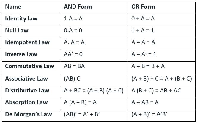
(A.A̅) + A
= 0 + A = A
All Boolean algebra laws are shown below:
A register capable of incrementing and/or decrementing its contents.- a)Counter
- b)Decoder
- c)Multiplexer
- d)Demultiplexer
Correct answer is option 'A'. Can you explain this answer?
A register capable of incrementing and/or decrementing its contents.
a)
Counter
b)
Decoder
c)
Multiplexer
d)
Demultiplexer
|
|
Sudhir Patel answered |
Concept:
- Flip-flop is a 1-bit memory cell which can be used for storing digital data.
- To increase the storage capacity in terms of the number of bits. A group of flip-flops is used. Such a group of flip-flops is known as a Register.
- A register capable of incrementing and/or decrementing its contents is called a counter
- A counter is a register capable of counting the number of clock pulses arriving at its clock input.
- A register is a group of flip-flops used to store multiple bits of data. An adder is a digital logic circuit in electronics that is extensively used for the addition of numbers.
- A latch is a circuit that has two stable states and can be used to store state information.
- The circuit can be made to change state by signals applied to one or more control inputs and will have one or two outputs.
Natural numbers are not closed under multiplication.- a)False
- b)True
- c)Cannot be determined
- d)None of these
Correct answer is option 'A'. Can you explain this answer?
Natural numbers are not closed under multiplication.
a)
False
b)
True
c)
Cannot be determined
d)
None of these
|
|
Sudhir Patel answered |
Concept:
The closure property of the multiplication of natural numbers states that the multiplication of two or more natural
numbers always result in a natural number.
numbers always result in a natural number.
Explanation:
Hence, two or more natural numbers multiplied results in a natural number.
For example, 5 × 2= 10, is a natural number.
Hence, two or more natural numbers multiplied results in a natural number.
For example, 5 × 2= 10, is a natural number.
Hence, the Correct answer is False.
Which among following is not a logic gate?- a)AND
- b)OR
- c)XR
- d)NOT
Correct answer is option 'C'. Can you explain this answer?
Which among following is not a logic gate?
a)
AND
b)
OR
c)
XR
d)
NOT
|
|
Sudhir Patel answered |
- XR is not an example of logic gates.
- Logic gates are the electronic circuit performing logical operations having one or more than one input and only one output.
- They works on the principle of Boolean function.
- The various examples of logic gates are AND Gate, OR Gate, NAND Gate, NOR Gate, XOR Gate, etc.
Chapter doubts & questions for Digital Logic - GATE Computer Science Engineering(CSE) 2026 Mock Test Series 2025 is part of Computer Science Engineering (CSE) exam preparation. The chapters have been prepared according to the Computer Science Engineering (CSE) exam syllabus. The Chapter doubts & questions, notes, tests & MCQs are made for Computer Science Engineering (CSE) 2025 Exam. Find important definitions, questions, notes, meanings, examples, exercises, MCQs and online tests here.
Chapter doubts & questions of Digital Logic - GATE Computer Science Engineering(CSE) 2026 Mock Test Series in English & Hindi are available as part of Computer Science Engineering (CSE) exam.
Download more important topics, notes, lectures and mock test series for Computer Science Engineering (CSE) Exam by signing up for free.
|
© EduRev
|
Education Revolution
|


|


Signup to see your scores
go up
within 7 days!
within 7 days!
Takes less than 10 seconds to signup