


All questions of Computer Architecture & Organisation (CAO) for Computer Science Engineering (CSE) Exam
Which of the following is not involved in a memory write operation?- a)MAR
- b)PC
- c)MDR
- d)data bus
Correct answer is option 'B'. Can you explain this answer?
Which of the following is not involved in a memory write operation?
a)
MAR
b)
PC
c)
MDR
d)
data bus
|
|
Ravi Singh answered |
Program counter register used to read the value or instruction not in write operation. For write operation MAR, IR and MDR registers are used.

In a C program, an array is declared as float A[2048]. Each array element is 4 Bytes in size, and the starting address of the array is 0x00000000. This program is run on a computer that has a direct mapped data cache of size 8 Kbytes, with block (line) size of 16 Bytes.
a. Which elements of the array conflict with element A[0] in the data cache? Justify your answer briefly.
b. If the program accesses the elements of this array one by one in reverse order i.e., starting with the last element and ending with the first element, how many data cache misses would occur? Justify your answer briefly. Assume that the data cache is initially empty and that no other data or instruction accesses are to be considered.Correct answer is '(a)'. Can you explain this answer?
In a C program, an array is declared as float A[2048]. Each array element is 4 Bytes in size, and the starting address of the array is 0x00000000. This program is run on a computer that has a direct mapped data cache of size 8 Kbytes, with block (line) size of 16 Bytes.
a. Which elements of the array conflict with element A[0] in the data cache? Justify your answer briefly.
b. If the program accesses the elements of this array one by one in reverse order i.e., starting with the last element and ending with the first element, how many data cache misses would occur? Justify your answer briefly. Assume that the data cache is initially empty and that no other data or instruction accesses are to be considered.
|
|
Ravi Singh answered |
(a)
Data cache size = 8KB.
Block line size = 16B.
Since each array element occupies 4B, four consecutive array elements occupy a block line (elements are aligned as
starting address is 0)
Number of cache blocks = 8KB/16B = 512. Number of cache blocks needed for the array = 2048/4 = 512. So, all the array
elements has its own cache block and there is no collision.
We can also explain this with respect to array address. Starting address is 0x00000000 = 0b0000..0 (32 0's). Ending
address is 0x00001FFF = 0b0000..0111111111111 (4*2048 = 8192 location).
Here, the last 4 bits are used as OFFSET bits and the next 9 bits are used as SET bits. So, since the ending address is not
extending beyond these 9 bits, all cache accesses are to diff sets.
(b) If the last element is accessed first, its cache block is fetched. (which should contain the previous 3 elements of the
array also since each cache block hold 4 elements of array and 2048 is and exact multiple of 4). Thus, for every 4
accesses, we will have a cache miss => for 2048 accesses we will have 512 cache misses. (This would be same even if we
access array in forward order).
Consider a three word machine instructionADD A[R0], @BThe first operand (destination) “A[R0]” uses indexed addressing mode with R0 as the index register. The second operand(source) “@B” uses indirect addressing mode. A and B are memory addresses residing at the second and third words,respectively. The first word of the instruction specifies the opcode, the index register designation and the source anddestination addressing modes. During execution of ADD instruction, the two operands are added and stored in thedestination (first operand).The number of memory cycles needed during the execution cycle of the instruction is:- a)3
- b)4
- c)5
- d)6
Correct answer is option 'B'. Can you explain this answer?
Consider a three word machine instruction
ADD A[R0], @B
The first operand (destination) “A[R0]” uses indexed addressing mode with R0 as the index register. The second operand(source) “@B” uses indirect addressing mode. A and B are memory addresses residing at the second and third words,respectively. The first word of the instruction specifies the opcode, the index register designation and the source anddestination addressing modes. During execution of ADD instruction, the two operands are added and stored in thedestination (first operand).
The number of memory cycles needed during the execution cycle of the instruction is:
a)
3
b)
4
c)
5
d)
6
|
|
Neha Choudhury answered |
In Indexed addressing mode, the base address is already in the instruction i.e A and to fetch the index data from R0 no memory access is required because it’s a register. So, to fetch the operand only 1 memory cycle is required.
Indirect Addressing mode requires 2 memory cycles only.
When we use auto increment or auto decrements, which of the following is/are true?
1) In both, the address is used to retrieve the operand and then the address gets altered
2) In auto increment the operand is retrieved first and then the address altered
3) Both of them can be used on general purpose registers as well as memory locations- a)1, 2, 3
- b)2
- c)1, 3
- d)2, 3
Correct answer is option 'D'. Can you explain this answer?
When we use auto increment or auto decrements, which of the following is/are true?
1) In both, the address is used to retrieve the operand and then the address gets altered
2) In auto increment the operand is retrieved first and then the address altered
3) Both of them can be used on general purpose registers as well as memory locations
1) In both, the address is used to retrieve the operand and then the address gets altered
2) In auto increment the operand is retrieved first and then the address altered
3) Both of them can be used on general purpose registers as well as memory locations
a)
1, 2, 3
b)
2
c)
1, 3
d)
2, 3
|
|
Yash Patel answered |
In the case of, auto increment the increment is done afterward and in auto decrement the decrement is done first.
Determine the width of Micro-instruction having following Control signal field, in a Vertical Microprogrammed Control Unit
1. Next Address field of 7 Bits
2. ALU Function field selecting 1 out of 13 ALU Function.
3. Register-in field selecting 1 out of 13 ALU Function.
4. Register-out field selecting 1 out of 8 registers.
5. Shifter field selecting no shift, right shift or left shift.
6. Auxiliary control field of 4 bits.- a)22
- b)23
- c)24
- d)25
Correct answer is option 'B'. Can you explain this answer?
Determine the width of Micro-instruction having following Control signal field, in a Vertical Microprogrammed Control Unit
1. Next Address field of 7 Bits
2. ALU Function field selecting 1 out of 13 ALU Function.
3. Register-in field selecting 1 out of 13 ALU Function.
4. Register-out field selecting 1 out of 8 registers.
5. Shifter field selecting no shift, right shift or left shift.
6. Auxiliary control field of 4 bits.
a)
22
b)
23
c)
24
d)
25
|
|
Shraddha Iyer answered |
Next Address Field = 7 Bits
ALU Function Field is of 4 Bits (to select possible 1 of 13 ALU fns)
Register-in and Register-out Fields of 3 Bits each Shifter Field of 2 bits to select 1 out of three possibilities:
Auxiliary Field of 4 Bits
Total Bits in μ-instruction
= 7 + 4 + 3 + 3 + 2 + 4 = 23
Register-in and Register-out Fields of 3 Bits each Shifter Field of 2 bits to select 1 out of three possibilities:
Auxiliary Field of 4 Bits
Total Bits in μ-instruction
= 7 + 4 + 3 + 3 + 2 + 4 = 23
The correct matching for the following pairs is:
(A) DMA I/O (1) High speed RAM
(B) Cache (2) Disk
(C) Interrupt I/O (3) Printer
(D) Condition Code Register (4) ALU
- a)A-4 B-3 C-1 D-2
- b)A-2 B-1 C-3 D-4
- c)A-4 B-3 C-2 D-1
- d)A-2 B-3 C-4 D-1
Correct answer is option 'B'. Can you explain this answer?
The correct matching for the following pairs is:
(A) DMA I/O (1) High speed RAM
(B) Cache (2) Disk
(C) Interrupt I/O (3) Printer
(D) Condition Code Register (4) ALU
(A) DMA I/O (1) High speed RAM
(B) Cache (2) Disk
(C) Interrupt I/O (3) Printer
(D) Condition Code Register (4) ALU
a)
A-4 B-3 C-1 D-2
b)
A-2 B-1 C-3 D-4
c)
A-4 B-3 C-2 D-1
d)
A-2 B-3 C-4 D-1

|
Machine Experts answered |
Explanation:
- DMA I/O (1) High speed RAM: DMA (Direct Memory Access) is used for transferring data between peripherals and memory without involving the CPU. It is commonly used for high-speed data transfers to and from high-speed RAM.
- Cache (2) Disk: Cache memory is a small, fast type of volatile computer memory used to temporarily store data that is frequently accessed. It helps in reducing the access time to data stored on slower storage devices like disks.
- Interrupt I/O (3) Printer: Interrupt I/O involves the use of interrupts to signal the CPU that a peripheral device needs attention. This is commonly used for devices like printers where the CPU needs to be informed when data is ready to be printed.
- Condition Code Register (4) ALU: The Condition Code Register (CCR) is a register used to store the condition codes generated by the ALU (Arithmetic Logic Unit) during arithmetic and logical operations. These codes are used to determine the outcome of operations and make decisions based on them.
The stage delays in a -stage pipeline are 800, 500, 400 and 300 picoseconds. The first stage (with delay 800 picoseconds) is replaced with a functionality equivalent design involving two stages with respective delays 600 and 350 picoseconds. The throughput increase of the pipeline is ___________ percent.Correct answer is '= 33.33%'. Can you explain this answer?
The stage delays in a -stage pipeline are 800, 500, 400 and 300 picoseconds. The first stage (with delay 800 picoseconds) is replaced with a functionality equivalent design involving two stages with respective delays 600 and 350 picoseconds. The throughput increase of the pipeline is ___________ percent.
|
|
Vaibhav Banerjee answered |
In pipeline ideally CPI = 1
So in 1 cycle 1 instruction gets completed
Throughout is instructions in unit time
In pipeline 1, cycle time = max stage delay = 800psec
In 800 * psec, we expect to finish 1 instuction
So, in 1s, 1/800 instructions are expected to be completed, which is also the throughput for pipeline 1.
Similarly pipeline 2, throughput = 1/600
Throughput increase in percentage
= 33.33%
Addressing mode is ______.- a)Explicitly specified
- b)Implied by the instruction
- c)Both (a) and (b)
- d)Neither (a) nor (b)
Correct answer is option 'C'. Can you explain this answer?
Addressing mode is ______.
a)
Explicitly specified
b)
Implied by the instruction
c)
Both (a) and (b)
d)
Neither (a) nor (b)
|
|
Tejas Ghoshal answered |
Addressing modes are either explicitly specified or implied by the instruction.
More than one word are put in one cache block to- a)exploit the temporal locality of reference in a program
- b)exploit the spatial locality of reference in a program
- c)reduce the miss penalty
- d)none of the above
Correct answer is option 'B'. Can you explain this answer?
More than one word are put in one cache block to
a)
exploit the temporal locality of reference in a program
b)
exploit the spatial locality of reference in a program
c)
reduce the miss penalty
d)
none of the above
|
|
Krish Datta answered |
exploit the spatial locality of reference in a program as, if the next locality is addressed immediately, it will already be in the cache.
Consider the scenario similar to cooking, where when an ingredient is taken from cupboard, you also take the near by ingredients along with it- hoping that they will be needed in near future.
Consider the scenario similar to cooking, where when an ingredient is taken from cupboard, you also take the near by ingredients along with it- hoping that they will be needed in near future.
Which of the following data transfer mode takes relatively more time?- a)DMA
- b)Interrupt initiated I/O
- c)Programmed I/O
- d)isolated I/O
Correct answer is option 'C'. Can you explain this answer?
Which of the following data transfer mode takes relatively more time?
a)
DMA
b)
Interrupt initiated I/O
c)
Programmed I/O
d)
isolated I/O
|
|
Jaya Chakraborty answered |
Programmed I/O data transfer mode takes relatively more time than DMA and interrupt initiated I/O.
Which of the following are NOT true in a pipelined processor?
I. Bypassing can handle all RAW hazards
II. Register renaming can eliminate all register carried WAR hazards
III. Control hazard penalties can be eliminated by dynamic branch prediction- a)I and II only
- b)I and III only
- c)II and III only
- d)I, II and III
Correct answer is option 'B'. Can you explain this answer?
Which of the following are NOT true in a pipelined processor?
I. Bypassing can handle all RAW hazards
II. Register renaming can eliminate all register carried WAR hazards
III. Control hazard penalties can be eliminated by dynamic branch prediction
I. Bypassing can handle all RAW hazards
II. Register renaming can eliminate all register carried WAR hazards
III. Control hazard penalties can be eliminated by dynamic branch prediction
a)
I and II only
b)
I and III only
c)
II and III only
d)
I, II and III
|
|
Aman Menon answered |
Pipelined Processor and Hazards
In a pipelined processor, instructions are divided into multiple stages and executed concurrently. This allows for improved performance by overlapping the execution of multiple instructions. However, this concurrent execution can introduce hazards, which are situations that prevent instructions from executing as intended. There are three types of hazards: data hazards, control hazards, and structural hazards.
I. Bypassing can handle all RAW hazards
Explanation:
- RAW (Read After Write) hazard occurs when a instruction depends on the result of a previous instruction that has not yet completed. This can lead to incorrect results if not handled properly.
- Bypassing, also known as forwarding, is a technique that allows data to be directly transferred from one stage of the pipeline to another without going through registers. It can help to resolve RAW hazards by providing the required data to instructions that need it.
- However, bypassing cannot handle all RAW hazards. There are situations where bypassing is not possible, such as when there are multiple dependent instructions in the pipeline or when the required data is not available in the pipeline.
- Therefore, the statement I is NOT true.
II. Register renaming can eliminate all register carried WAR hazards
Explanation:
- WAR (Write After Read) hazard occurs when a instruction writes to a register that is later read by another instruction before the write operation completes. This can lead to incorrect results if not handled properly.
- Register renaming is a technique that assigns multiple physical registers to the same logical register, allowing instructions to write to and read from different physical registers. This eliminates WAR hazards by ensuring that the read operation gets the correct value from the renamed register.
- However, there are situations where register renaming cannot eliminate WAR hazards, such as when there are dependencies between instructions that cannot be resolved by renaming registers.
- Therefore, the statement II is NOT true.
III. Control hazard penalties can be eliminated by dynamic branch prediction
Explanation:
- Control hazards occur when the control flow of the program is altered due to branches, jumps, or other control transfer instructions. This can lead to pipeline stalls and reduced performance.
- Dynamic branch prediction is a technique that predicts the outcome of branch instructions based on the behavior of previous branches. It allows the pipeline to continue executing instructions speculatively based on the predicted outcome.
- While dynamic branch prediction can significantly reduce the penalties associated with control hazards, it cannot eliminate them entirely. There are cases where the prediction may be incorrect, leading to incorrect execution and the need to flush the pipeline.
- Therefore, the statement III is NOT true.
Conclusion
- In summary, the correct answer is option 'B' because statements II and III are NOT true in a pipelined processor. Bypassing cannot handle all RAW hazards, and register renaming cannot eliminate all register carried WAR hazards. Similarly, while dynamic branch prediction can reduce control hazard penalties, it cannot eliminate them entirely.
If M denotes the number of memory locations and N denotes the word size, then an expression that denotes the storage capacity is ______________- a)M * N
- b)M + N
- c)2M + N
- d)2M - N
Correct answer is option 'A'. Can you explain this answer?
If M denotes the number of memory locations and N denotes the word size, then an expression that denotes the storage capacity is ______________
a)
M * N
b)
M + N
c)
2M + N
d)
2M - N
|
|
Sudhir Patel answered |
Storage capacity is the product of a number of memory locations that is the number of words and the word size or the number of bits stored per location. Storage capacity should be as large as possible.
Consider the unpipelined machine with 10 ns clock cycles. It uses four cycles for ALU operations and branches, whereas five cycles for memory operations. Assume that the relative frequencies of there operations are 40%, 20%, 40% respectively. Suppose that due to clock skew and setup, pipelining the machine adds 1 ns overhead to the clock. How much speed up in the instruction execution rate will we gain from a pipeline?
- a)5 times
- b)4 times
- c)8 times
- d)4.5 times
Correct answer is option 'B'. Can you explain this answer?
Consider the unpipelined machine with 10 ns clock cycles. It uses four cycles for ALU operations and branches, whereas five cycles for memory operations. Assume that the relative frequencies of there operations are 40%, 20%, 40% respectively. Suppose that due to clock skew and setup, pipelining the machine adds 1 ns overhead to the clock. How much speed up in the instruction execution rate will we gain from a pipeline?
a)
5 times
b)
4 times
c)
8 times
d)
4.5 times
|
|
Subham Saha answered |
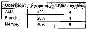
Total clock cycle
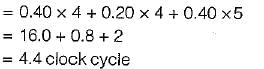
Under non pipeline time = 4.4 x (10) = 44
Under pipeline time
= 10 + overhead = 10 + 1 = 11
So, speedup = 44/11 = 4 times
A processor that communicates with remote terminals over telephone and other communication media in a serial fashion is called _______ .- a)I/O processor
- b)DMA controller
- c)Data communication processor
- d)USART
Correct answer is option 'D'. Can you explain this answer?
A processor that communicates with remote terminals over telephone and other communication media in a serial fashion is called _______ .
a)
I/O processor
b)
DMA controller
c)
Data communication processor
d)
USART

|
Sanmit Vartak answered |
Data communication processor is the processor that communicate with remote terminals over telephone and other communication media in a serial fashion.
Which of the following addressing modes permits relocation without any change whatsoever in the code?
- a)Indirect addressing
- b)Indexed addressing
- c)PC relative addressing
- d)PC relative addressing
Correct answer is option 'D'. Can you explain this answer?
Which of the following addressing modes permits relocation without any change whatsoever in the code?
a)
Indirect addressing
b)
Indexed addressing
c)
PC relative addressing
d)
PC relative addressing

|
Swara Dasgupta answered |
PC relative addressing mode:
The effective memory address is obtained by computing an offset from the current PC. No matter where the code is loaded in memory, the offsets are always the same so the code needs no modification. In this addressing, there is absolutely no change in code needed.
Therefore the answer is Option 4 i.e, PC relative Addressing
The performance of a pipelined processor suffers if _______.- a)The pipeline stages have different delays.
- b)Consecutive instructions are dependent on each other.
- c)The pipeline stages share hardware resources,
- d)All of these
Correct answer is option 'D'. Can you explain this answer?
The performance of a pipelined processor suffers if _______.
a)
The pipeline stages have different delays.
b)
Consecutive instructions are dependent on each other.
c)
The pipeline stages share hardware resources,
d)
All of these
|
|
Sonal Nair answered |
The performance of a pipelined processor depends upon delays of different stage and its hardware resources also it depends upon consecutive instructions format.
Consider a processor with 64 registers and an instruction set of size twelve. Each instruction has five distinct fields, namely, opcode, two source register identifiers, one destination register identifier, and twelve-bit immediate value. Each instruction must be stored in memory in a byte-aligned fashion. If a program has 100 instructions, the amount of memory (in bytes)
consumed by the program text is _________.Correct answer is '=> 500 bytes'. Can you explain this answer?
Consider a processor with 64 registers and an instruction set of size twelve. Each instruction has five distinct fields, namely, opcode, two source register identifiers, one destination register identifier, and twelve-bit immediate value. Each instruction must be stored in memory in a byte-aligned fashion. If a program has 100 instructions, the amount of memory (in bytes)
consumed by the program text is _________.
consumed by the program text is _________.
|
|
Ameya Goyal answered |
Answer => 500 bytes
Number of register = 64
Number of bits to address register = [log264] = 6 bits
Number of Instruction = 12
Opcode size = [log212] = 4
Opcode(4) reg1(6) reg2(6) reg2(6) Immediate(12)
Total bits per instruction = 34
Total bytes per instruction= 4.25
Due to byte alignment we cannot store 4.25 bytes, without wasting 0.75 bytes ,
So Total bytes per instruction = 5
Total instruction = 100
Total size = Number of instruction x Size of instruction 100 x 5= 500 Byes
The main memory of a computer has 2 cm blocks while the cache has 2c blocks. If the cache uses the set associativemapping scheme with 2 blocks per set, then block k of the main memory maps to the set- a)(k mod m) of the cache
- b)(k mod c) of the cache
- c)(k mod 2c) of the cache
- d)(k mod 2 cm) of the cache
Correct answer is option 'B'. Can you explain this answer?
The main memory of a computer has 2 cm blocks while the cache has 2c blocks. If the cache uses the set associativemapping scheme with 2 blocks per set, then block k of the main memory maps to the set
a)
(k mod m) of the cache
b)
(k mod c) of the cache
c)
(k mod 2c) of the cache
d)
(k mod 2 cm) of the cache
|
|
Janani Joshi answered |
Main Memory and Cache Structure
In a computer system, the organization of memory is crucial for performance. The main memory consists of blocks, and in this scenario, it has 2 cm blocks. The cache, which is faster and smaller, contains 2c blocks.
Cache Mapping Scheme
The cache employs a set associative mapping scheme with 2 blocks per set. This means that the cache can hold multiple blocks from the main memory in each set, allowing for more flexibility and faster access.
Understanding Block Mapping
To determine where a block from main memory maps in the cache, we can use the formula for set indexing. The formula typically involves the total number of cache blocks and the number of sets. Here’s how to analyze it:
- Total cache blocks: 2c
- Number of sets: Since there are 2 blocks per set, the number of sets in the cache = (2c) / 2 = c.
Now, to find out which set a block k from main memory maps to:
- Mapping formula: Block k will map to a set in the cache based on the modulo operation with the number of sets.
Calculating the Set Index
Since we have c sets, the formula to find the set for block k is:
- Set index = k mod c
This is because c is the number of sets in the cache, and using modulo c will provide the correct set index for the block.
Conclusion
Thus, the correct answer to where block k of the main memory maps in the cache is option b) (k mod c) of the cache. Understanding this mapping is crucial for optimizing cache performance in computer systems.
Which of the following is the fastest memory?- a)Cache Memory
- b)DVD ROMs
- c)Static RAM
- d)Hard Disk
Correct answer is option 'A'. Can you explain this answer?
Which of the following is the fastest memory?
a)
Cache Memory
b)
DVD ROMs
c)
Static RAM
d)
Hard Disk

|
G.K Academy answered |
- Cache memory is a special very high-speed memory.
- It is used to speed up and synchronize with the high-speed CPU. Cache memory is more expensive than main memory or disk memory but economical as compared to CPU registers.
- Cache memory is an extremely fast memory type that acts as a buffer between the RAM and the CPU.
- It holds frequently requested data and instructions so that they are immediately available to the CPU when needed.
- Cache memory is used to reduce the average time to access data from the main memory.
System calls are usually invoked by using
1. An indirect jump
2. A software interrupt
3. Polling
4. A privileged instruction- a)2 and 3
- b)1 and 3
- c)1, 2, 3 and 4
- d)3 and 4
Correct answer is option 'A'. Can you explain this answer?
System calls are usually invoked by using
1. An indirect jump
2. A software interrupt
3. Polling
4. A privileged instruction
1. An indirect jump
2. A software interrupt
3. Polling
4. A privileged instruction
a)
2 and 3
b)
1 and 3
c)
1, 2, 3 and 4
d)
3 and 4
|
|
Harshitha Banerjee answered |
System call is a request in unit like operating system made via software interrupt by an active process for a service performed by the Kernal.
Consider a pipelined processor with the following four stages: - IF: Instruction Fetch
- ID: Instruction Decode and Operand Fetch
- EX: Execute
- WB: Write Back
The IF, ID and WB stages take one clock cycle each to complete the operation. The number of clock cycles for the EX stage depends on the instruction. The ADD and SUB instructions need 1 clock cycle and the MUL instruction needs 3 clock cycles in the EX stage. Operand forwarding is used in the pipelined processor. What is the number of clock cycles taken to complete the following sequence of instructions?
ADD R2, R1, R0 R2 ← R1 + R0
MUL R4, R3, R2 R4 ← R3 * R2
SUB R6, R5, R4 R6 ← R5 - R4- a)7
- b)8
- c)10
- d)14
Correct answer is option 'B'. Can you explain this answer?
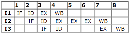
Consider a pipelined processor with the following four stages:
- IF: Instruction Fetch
- ID: Instruction Decode and Operand Fetch
- EX: Execute
- WB: Write Back
The IF, ID and WB stages take one clock cycle each to complete the operation. The number of clock cycles for the EX stage depends on the instruction. The ADD and SUB instructions need 1 clock cycle and the MUL instruction needs 3 clock cycles in the EX stage. Operand forwarding is used in the pipelined processor. What is the number of clock cycles taken to complete the following sequence of instructions?
ADD R2, R1, R0 R2 ← R1 + R0
MUL R4, R3, R2 R4 ← R3 * R2
SUB R6, R5, R4 R6 ← R5 - R4
ADD R2, R1, R0 R2 ← R1 + R0
MUL R4, R3, R2 R4 ← R3 * R2
SUB R6, R5, R4 R6 ← R5 - R4
a)
7
b)
8
c)
10
d)
14
|
|
Prerna Joshi answered |
Answer: option B
considering EX to EX data forwarding.
considering EX to EX data forwarding.
A non pipelined single cycle processor operating at 100 MHz is converted into a synchronous pipelined processor with five stages requiring 2.5 nsec, 1.5 nsec, 2 nsec, 1.5 nsec and 2.5 nsec, respectively. The delay of the latches is 0.5 nsec. The speedup of the pipeline processor for a large number of instructions is- a)4.5
- b)4.0
- c)3.33
- d)3.0
Correct answer is option 'C'. Can you explain this answer?
A non pipelined single cycle processor operating at 100 MHz is converted into a synchronous pipelined processor with five stages requiring 2.5 nsec, 1.5 nsec, 2 nsec, 1.5 nsec and 2.5 nsec, respectively. The delay of the latches is 0.5 nsec. The speedup of the pipeline processor for a large number of instructions is
a)
4.5
b)
4.0
c)
3.33
d)
3.0
|
|
Sarthak Desai answered |
Given Information:
- Non-pipelined single cycle processor operates at 100 MHz.
- Synchronous pipelined processor has five stages with the following delays:
- Stage 1: 2.5 nsec
- Stage 2: 1.5 nsec
- Stage 3: 2 nsec
- Stage 4: 1.5 nsec
- Stage 5: 2.5 nsec
- Delay of the latches is 0.5 nsec.
Calculating Speedup:
The speedup of the pipelined processor can be calculated using the formula:
Speedup = Non-pipelined processor time / Pipelined processor time
Non-pipelined Processor Time:
The non-pipelined processor operates at 100 MHz, which means each instruction takes 1 / 100 MHz = 10 nsec to complete.
Pipelined Processor Time:
The pipelined processor has five stages with the following delays:
- Stage 1: 2.5 nsec
- Stage 2: 1.5 nsec
- Stage 3: 2 nsec
- Stage 4: 1.5 nsec
- Stage 5: 2.5 nsec
Additionally, there is a delay of 0.5 nsec for each latch.
To calculate the pipelined processor time, we need to consider the longest stage delay, which is 2.5 nsec for Stage 1. Therefore, the pipelined processor time is 2.5 nsec + 0.5 nsec = 3 nsec.
Speedup Calculation:
Speedup = Non-pipelined processor time / Pipelined processor time
= 10 nsec / 3 nsec
≈ 3.33
Therefore, the speedup of the pipeline processor for a large number of instructions is approximately 3.33.
Answer:
The correct answer is option C) 3.33.
Cache memory is the onboard storage.- a)True
- b)False
- c)Can't be Determined
- d)None of Above
Correct answer is option 'A'. Can you explain this answer?
Cache memory is the onboard storage.
a)
True
b)
False
c)
Can't be Determined
d)
None of Above
|
|
Sudhir Patel answered |
Cache Memory is the memory closest to the CPU. Registers, Cache and the main memory are the means of onboard storage in the computer system.
Consider a 6-stage instruction pipeline, where all stages are perfectly balanced. Assume that there is no cycle-time overhead of pipelining. When an application is executing on this 6-stage pipeline, the speedup achieved with respect to non-pipelined execution if 25% of the instructions incur 2 pipeline stall cycles is ____________Correct answer is '4'. Can you explain this answer?
Consider a 6-stage instruction pipeline, where all stages are perfectly balanced. Assume that there is no cycle-time overhead of pipelining. When an application is executing on this 6-stage pipeline, the speedup achieved with respect to non-pipelined execution if 25% of the instructions incur 2 pipeline stall cycles is ____________
|
|
Vaibhav Banerjee answered |
Time without pipeline = 6 stages=6 cycles
Time with pipeline =1+stall freqency*stall cycle
=1+.25*2
=1.5
Time with pipeline =1+stall freqency*stall cycle
=1+.25*2
=1.5
Speed up = 6/1.5
=4
=4
Comparing the time T1 taken for a single instruction on a pipelined CPU with time T2 taken on a non-pipelined but identicalCPU, we can say that- a)T1 ≤ T2
- b)T1 ≥ T2
- c)T1 < T2
- d)T1 and T2 plus the time taken for one instruction fetch cycle
Correct answer is option 'B'. Can you explain this answer?
Comparing the time T1 taken for a single instruction on a pipelined CPU with time T2 taken on a non-pipelined but identicalCPU, we can say that
a)
T1 ≤ T2
b)
T1 ≥ T2
c)
T1 < T2
d)
T1 and T2 plus the time taken for one instruction fetch cycle
|
|
Aarav Malik answered |
Here we are comparing the execution time of only a single instruction. Pipelining in no way increases the execution time of a single instruction (the time from its start to end). It increases the overall performance by splitting the execution to multiple pipeline stages so that the following instructions can use the finished stages of the previous instructions. But in doing so pipelining causes some problems also as given in the below link, which might slow some instructions. So, (B) is the answer.
A pipelined processor uses a 4-stage instruction pipeline with the following stages: Instruction fetch (IF), Instruction decode (ID), Execute (EX) and Writeback (WB). The arithmetic operations as well as the load and store operations are carried out in the EX stage. The sequence of instructions corresponding to the statement X = (S - R * (P + Q))/T is given below. The values of variables P, Q, R, S and T are available in the registers R0, R1, R2, R3 and R4 respectively, before the execution of the instruction sequence.
ADD R5, R0, R1 ; R5 → R0 + R1
MUL R6, R2, R5 ; R6 → R2 * R5
SUB R5, R3, R6 ; R5 → R3 - R6
DIV R6, R5, R4 ; R6 → R5/R4
STORE R6, X ; X ← R6
The IF, ID and WB stages take 1 clock cycle each. The EX stage takes 1 clock cycle each for the ADD, SUB and STORE operations, and 3 clock cycles each for MUL and DIV operations. Operand forwarding from the EX stage to the ID stage is used. The number of clock cycles required to complete the sequence of instructions is- a)10
- b)12
- c)14
- d)16
Correct answer is option 'B'. Can you explain this answer?
A pipelined processor uses a 4-stage instruction pipeline with the following stages: Instruction fetch (IF), Instruction decode (ID), Execute (EX) and Writeback (WB). The arithmetic operations as well as the load and store operations are carried out in the EX stage. The sequence of instructions corresponding to the statement X = (S - R * (P + Q))/T is given below. The values of variables P, Q, R, S and T are available in the registers R0, R1, R2, R3 and R4 respectively, before the execution of the instruction sequence.
ADD R5, R0, R1 ; R5 → R0 + R1
MUL R6, R2, R5 ; R6 → R2 * R5
SUB R5, R3, R6 ; R5 → R3 - R6
DIV R6, R5, R4 ; R6 → R5/R4
STORE R6, X ; X ← R6
The IF, ID and WB stages take 1 clock cycle each. The EX stage takes 1 clock cycle each for the ADD, SUB and STORE operations, and 3 clock cycles each for MUL and DIV operations. Operand forwarding from the EX stage to the ID stage is used. The number of clock cycles required to complete the sequence of instructions is
a)
10
b)
12
c)
14
d)
16
|
|
Pallabi Sharma answered |
Understanding the Pipelined Execution
In a 4-stage pipelined processor, we have the following stages: Instruction Fetch (IF), Instruction Decode (ID), Execute (EX), and Writeback (WB). Each stage takes 1 clock cycle, except for MUL and DIV, which take 3 cycles.
Instruction Breakdown
1. ADD R5, R0, R1
- Takes 1 cycle in IF, ID, EX, and 1 cycle in WB (Total: 4 cycles).
2. MUL R6, R2, R5
- Takes 1 cycle in IF, ID, 3 cycles in EX, and 1 cycle in WB (Total: 6 cycles).
3. SUB R5, R3, R6
- Takes 1 cycle in IF, ID, EX, and 1 cycle in WB (Total: 4 cycles).
4. DIV R6, R5, R4
- Takes 1 cycle in IF, ID, 3 cycles in EX, and 1 cycle in WB (Total: 6 cycles).
5. STORE R6, X
- Takes 1 cycle in IF, ID, EX, and 1 cycle in WB (Total: 4 cycles).
Pipelining and Clock Cycles
- The pipeline can overlap the execution of instructions.
- Each instruction progresses through the stages simultaneously, and the total cycles will be determined by the longest EX stage.
Cycle Calculation
- The critical path is defined by the longest operation, which is MUL (6 cycles) and DIV (6 cycles).
- Thus, the total number of clock cycles required to complete all instructions is determined by the longest EX stages, plus the time taken for the first instruction to complete its WB stage.
Total Clock Cycle Count
- The total clock cycles required:
- 1 (IF for ADD) + 1 (ID for ADD) + 1 (EX for ADD) + 1 (WB for ADD)
- + 1 (IF for MUL, overlaps with ID for ADD)
- + 1 (ID for MUL) + 3 (EX for MUL) + 1 (WB for MUL)
- + 1 (IF for SUB, overlaps with ID for MUL)
- + 1 (ID for SUB) + 1 (EX for SUB) + 1 (WB for SUB)
- + 1 (IF for DIV, overlaps with ID for SUB)
- + 1 (ID for DIV) + 3 (EX for DIV) + 1 (WB for DIV)
- + 1 (IF for STORE, overlaps with ID for DIV)
- + 1 (ID for STORE) + 1 (EX for STORE) + 1 (WB for STORE)
The total comes up to 12 cycles.
Thus, the correct answer is 12 cycles (option b).
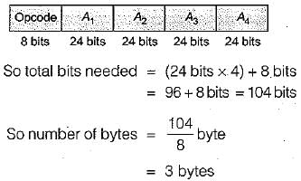
In four-address instruction format, the number of bytes required to encode an instruction is (assume each address requires 24 bits, and 1 byte is required for operation code)- a)9
- b)13
- c)14
- d)12
Correct answer is option 'B'. Can you explain this answer?
In four-address instruction format, the number of bytes required to encode an instruction is (assume each address requires 24 bits, and 1 byte is required for operation code)
a)
9
b)
13
c)
14
d)
12
|
|
Mahi Yadav answered |
Four address instruction format:
An instruction pipeline consists of 4 stages – Fetch (F), Decode field (D), Execute (E) and Result Write (W). The 5 instructions in a certain instruction sequence need these stages for the different number of clock cycles as shown by the table below
No. of cycles needed for
Instruction F D E W
1 1 2 1 1
2 1 2 2 1
3 2 1 3 2
4 1 3 2 1
5 1 2 1 2
Find the number of clock cycles needed to perform the 5 instructions.Correct answer is '15 cycles are required.'. Can you explain this answer?
An instruction pipeline consists of 4 stages – Fetch (F), Decode field (D), Execute (E) and Result Write (W). The 5 instructions in a certain instruction sequence need these stages for the different number of clock cycles as shown by the table below
No. of cycles needed for
Instruction F D E W
1 1 2 1 1
2 1 2 2 1
3 2 1 3 2
4 1 3 2 1
5 1 2 1 2
Find the number of clock cycles needed to perform the 5 instructions.
No. of cycles needed for
Instruction F D E W
1 1 2 1 1
2 1 2 2 1
3 2 1 3 2
4 1 3 2 1
5 1 2 1 2
Find the number of clock cycles needed to perform the 5 instructions.
|
|
Jatin Joshi answered |
answer = 15 cycles are required.

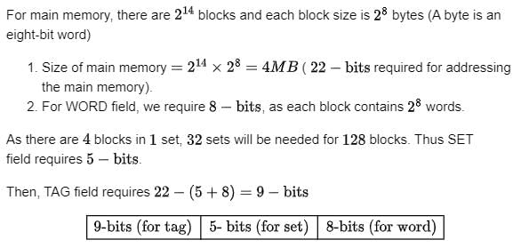
A block-set associative cache memory consists of 128 blocks divided into four block sets. The main memory consists of 16,384 blocks and each block contains 256 eight bit words.
- How many bits are required for addressing the main memory?
- How many bits are needed to represent the TAG, SET and WORD fields?
Correct answer is '9'. Can you explain this answer?
A block-set associative cache memory consists of 128 blocks divided into four block sets. The main memory consists of 16,384 blocks and each block contains 256 eight bit words.
- How many bits are required for addressing the main memory?
- How many bits are needed to represent the TAG, SET and WORD fields?
|
|
Bibek Chakraborty answered |
The CPU initializes the DMA by sending ______ .- a)The starting address of the memory blocks where data is available or where data is to be stored.
- b)The word count.
- c)Control for mode and start the transfer.
- d)All of these
Correct answer is option 'D'. Can you explain this answer?
The CPU initializes the DMA by sending ______ .
a)
The starting address of the memory blocks where data is available or where data is to be stored.
b)
The word count.
c)
Control for mode and start the transfer.
d)
All of these
|
|
Soumya Dey answered |
The CPU initializes the DMA by sending:
The starting address of the memory blocks where data are available (for read) or where data are to be stored. (For write)
The word count, which is the number of words in the memory.
Control to specify the mode of transfer such as read or write.
The starting address of the memory blocks where data are available (for read) or where data are to be stored. (For write)
The word count, which is the number of words in the memory.
Control to specify the mode of transfer such as read or write.
An instruction pipeline has five stages where each stage take 2 nanoseconds and all instruction use all five stages. Branch instructions are not overlapped. i.e., the instruction after the branch is not fetched till the branch instruction is completed. Under ideal conditions,
a. Calculate the average instruction execution time assuming that 20% of all instructions executed are branch instruction. Ignore the fact that some branch instructions may be conditional.
b. If a branch instruction is a conditional branch instruction, the branch need not be taken. If the branch is not taken, the following instructions can be overlapped. When 80% of all branch instructions are conditional branch instructions, and 50% of the conditional branch instructions are such that the branch is taken, calculate the average instruction execution time.Correct answer is 'Each stage is 2 ns.'. Can you explain this answer?
An instruction pipeline has five stages where each stage take 2 nanoseconds and all instruction use all five stages. Branch instructions are not overlapped. i.e., the instruction after the branch is not fetched till the branch instruction is completed. Under ideal conditions,
a. Calculate the average instruction execution time assuming that 20% of all instructions executed are branch instruction. Ignore the fact that some branch instructions may be conditional.
b. If a branch instruction is a conditional branch instruction, the branch need not be taken. If the branch is not taken, the following instructions can be overlapped. When 80% of all branch instructions are conditional branch instructions, and 50% of the conditional branch instructions are such that the branch is taken, calculate the average instruction execution time.
|
|
Jatin Joshi answered |
Each stage is 2ns. So, after 5 time units each of 2ns, the first instruction finishes (i.e., after 10ns), in every 2ns after that a new instruction gets finished. This is assuming no branch instructions. Now, once the pipeline is full, we can assume that the initial fill time doesn't matter our calculations and average execution time for each instruction is 2ns assuming no
branch instructions.
(a) Now, we are given that 20% of instructions are branch (like JMP) and when a branch instruction is executed, no further instruction enters the pipeline. So, we can assume every 5th instruction is a branch instruction. So, with this assumption, total time to finish 5 instruction will be 5 * 2 + 8 = 18 ns (as when a branch instruction enters the pipeline and before it finishes, 4 pipeline stages will be empty totaling 4 * 2 = 8 ns, as it is mentioned in question that the next instruction fetch starts only when branch instruction completes). And this is the same for every set of 5 instructions, and hence the average instruction execution time = 18/5 = 3.6 ns
(b) This is just a complex statement. But what we need is to identify the % of branch instructions which cause a branch to be taken as others will have no effect on the pipeline flow.
20% of branch instructions are branch instructions. 80% of branch instructions are conditional.
That means .2*.8 = 16% of instructions are conditional branch instructions and it is given that 50% of those result in a branch being taken.
So, 8% of instructions are conditional branches being taken and we also have 20% of 20% = 4% of unconditional branch
instructions which are always taken.
So, percentage of instructions where a branch is taken is 8+4 = 12% instead of 20% in (a) part.
So, in 100 instructions there will be 12 branch instructions. We can do a different calculation here as compared to (a) as 12 is not a divisor of 100. Each branch instruction causes a pipeline delay of 4*2 = 8 ns. So, 12 instructions will cause a
delay of 12 * 8 = 96 ns. For 100 instructions, we need 100 * 2 = 200 ns without any delay and with delay we require 200 + 96 = 296 ns for 100 instructions.
So, average instruction execution time = 296/100 = 2.96 ns (We can also use this method for part (a) which will give 100 * 2 + 20*8 = 360 ns for 100 instructions)
Which among the following memories is used in Digital camera?- a)Flash memory
- b)Virtual memory
- c)Main memory
- d)Cache memory
Correct answer is option 'A'. Can you explain this answer?
Which among the following memories is used in Digital camera?
a)
Flash memory
b)
Virtual memory
c)
Main memory
d)
Cache memory
|
|
G.K Academy answered |
- Digital Camera
- It is a camera that captures photographs in flash memory.
- The basis for digital camera image sensors is metal-oxide-semiconductor technology.
- Steven Sasson invented the world's first digital camera in 1975.
- Flash Memory
- It is a type of nonvolatile memory that erases data in units called blocks and rewrites data at the byte level.
- It is widely used for storage and data transfers in consumer devices, industrial applications.
- Flash memory is a non-volatile computer storage chip,
- It is made up of EEPROM.
- EEPROM is the acronym of electrically erasable programmable read-only memory,
- EEPROM is a Programmable ROM that can be erased and reprogrammed using an electrical charge.
- It was first was developed by George Perlegos.
- It allows the user to update the computer BIOS without having to open the computer or remove any chips.
- It is organized as arrays of floating-gate transistors.
- USB flash drives, Memory cards are examples of flash memory storage.
- BIOS is stored in a Flash memory chip.
Consider two cache organizations. First one is 32 kb 2-way set associative with 32 byte block size, the second is of same size but direct mapped. The size of an address is 32 bits in both cases . A 2-to-1 multiplexer has latency of 0.6 ns while a k - bit comparator has latency ofk/10 ns The hit latency of the set associative organization is h1 while that of direct mapped is h2
.
The value of h1 is:- a)2.4 ns
- b)2.3 ns
- c)1.8 ns
- d)1.7 ns
Correct answer is option 'A'. Can you explain this answer?
Consider two cache organizations. First one is 32 kb 2-way set associative with 32 byte block size, the second is of same size but direct mapped. The size of an address is 32 bits in both cases . A 2-to-1 multiplexer has latency of 0.6 ns while a k - bit comparator has latency of
k/10 ns The hit latency of the set associative organization is h1 while that of direct mapped is h2
.
The value of h1 is:
.
The value of h1 is:
a)
2.4 ns
b)
2.3 ns
c)
1.8 ns
d)
1.7 ns
|
|
Prashanth Patel answered |
Cache size is 32 KB and cache block size is 32 B. So,
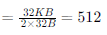
So, number of index bits needed = 9 ( since 29 = 512). Number of offset bits = 5 (since 25 = 32 B is the block size and assuming byte addressing). So, number of tag bits = 32 - 9 - 5 = 18 (as memory address is of 32 bits).
So, time for comparing the data = Time to compare the data + Time to select the block in set = 0.6 + 18/10 ns = 2.4 ns.
(Two comparisons of tag bits need to be done for each block in a set, but they can be carried out in parallel and the succeeding one multiplexed as the output).
Relative mode of addressing is most relevant to writing- a)Co-routines
- b)Position – independent code
- c)Shareable code
- d)Interrupt Handlers
Correct answer is option 'B'. Can you explain this answer?
Relative mode of addressing is most relevant to writing
a)
Co-routines
b)
Position – independent code
c)
Shareable code
d)
Interrupt Handlers
|
|
Pranab Banerjee answered |
Answer: B
Relative mode addressing is most relevant to writing a position-independent code.
Relative mode addressing is most relevant to writing a position-independent code.
Booth's algorithm is used in floating-point- a)Addition
- b)Subtraction
- c)Multiplication
- d)Division
Correct answer is option ''. Can you explain this answer?
Booth's algorithm is used in floating-point
a)
Addition
b)
Subtraction
c)
Multiplication
d)
Division
|
|
Shruti Basak answered |
Booth’s algorithm is used for floating point multiplication.
The principle of locality justifies the use of- a)Interrupts
- b)DMA
- c)Polling
- d)Cache Memory
Correct answer is option 'D'. Can you explain this answer?
The principle of locality justifies the use of
a)
Interrupts
b)
DMA
c)
Polling
d)
Cache Memory
|
|
Mahesh Pillai answered |
It is D.
Locality of reference is actually the frequent accessing of any storage location or some value. We can say in simple language that whatever things are used more frequently, they are stored in the locality of reference. So we have cache memory for the purpose.
Locality of reference is actually the frequent accessing of any storage location or some value. We can say in simple language that whatever things are used more frequently, they are stored in the locality of reference. So we have cache memory for the purpose.
Consider the following situation and fill in the blanks:The computer starts the tape moving by issuing a command: the processor then monitors the status of the tape by means of a _____. When the tape is in the correct position, the processor issues a _______.- a)Data input, status, data output command
- b)Data input, status control command
- c)Control, status, data output command
- d)Control, status, data input command
Correct answer is option 'C'. Can you explain this answer?
Consider the following situation and fill in the blanks:
The computer starts the tape moving by issuing a command: the processor then monitors the status of the tape by means of a _____. When the tape is in the correct position, the processor issues a _______.
a)
Data input, status, data output command
b)
Data input, status control command
c)
Control, status, data output command
d)
Control, status, data input command
|
|
Bijoy Sharma answered |
Control command: A control command is issued to activate the peripheral and to inform it what to do.
Status: A status command is used to test various status conditions in the interface and the peripheral.
Data output command causes the interface to respond by transferring data from the bus into one of its register.
Status: A status command is used to test various status conditions in the interface and the peripheral.
Data output command causes the interface to respond by transferring data from the bus into one of its register.
The following are four statements about Reduced Instruction Set Computer (RISC) architectures.
1. The typical RISC machine instruction set is small, and is usually a subject of a CISC instruction set.
2. No arithmetic or logical instruction can refer to the memory directly.
3. A comparatively large number of user registers are available.
4. Instructions can be easily decoded through hard-wired control units.Which of the above statements is true?- a)1 and 3 only
- b)1,3 and 4 only
- c)1, 2 and 3 only
- d)All of these
Correct answer is option 'D'. Can you explain this answer?
The following are four statements about Reduced Instruction Set Computer (RISC) architectures.
1. The typical RISC machine instruction set is small, and is usually a subject of a CISC instruction set.
2. No arithmetic or logical instruction can refer to the memory directly.
3. A comparatively large number of user registers are available.
4. Instructions can be easily decoded through hard-wired control units.
Which of the above statements is true?
a)
1 and 3 only
b)
1,3 and 4 only
c)
1, 2 and 3 only
d)
All of these
|
|
Janani Joshi answered |
Reduced instruction set uses comparatively large number of user registers, all arithmetic or logical instruction refer to memory via registers only, instructions can be easily decoded through hardwired control unit and is small instruction set and is usually a subject of a CISI instruction set
The disadvantage of hard-wired control units with flip-flops is ______.- a)Design becomes complex
- b)It require more number of flip-flops
- c)Control circuit speed does not matches with flip-flops
- d)None of these
Correct answer is option 'B'. Can you explain this answer?
The disadvantage of hard-wired control units with flip-flops is ______.
a)
Design becomes complex
b)
It require more number of flip-flops
c)
Control circuit speed does not matches with flip-flops
d)
None of these
|
|
Meghana Rane answered |
The disadvantage of hardwired control units with flip-flops is that it requires more number of flip- flops.
______ is a piece of hardware that executes a set of machine-language instructions.- a)Controller
- b)Bus
- c)Processor
- d)Motherboard
Correct answer is option 'C'. Can you explain this answer?
______ is a piece of hardware that executes a set of machine-language instructions.
a)
Controller
b)
Bus
c)
Processor
d)
Motherboard
|
|
Ipsita Dasgupta answered |
Processor or processing unit is an electronic CKT which perform operations on some external source, usually memory or some data stream. Processor executes a set of machine language instructions.
To prevent signals, from colliding on the bus, _______ prioritize access to memory by I/O channels and processors.- a)A register
- b)Interrupts '
- c)The processor scheduler
- d)A controller
Correct answer is option 'D'. Can you explain this answer?
To prevent signals, from colliding on the bus, _______ prioritize access to memory by I/O channels and processors.
a)
A register
b)
Interrupts '
c)
The processor scheduler
d)
A controller
|
|
Megha Dasgupta answered |
To prevent signals from colliding on the bus, a controller prioritize access to memory by I/O channels and processors.
A device with data transfer rate 10 KB/sec is connected to a CPU. Data is transferred byte- wise. Let the interrupt overhead be 4 μsec. The byte transfer time between the device interface register and CPU or memory is negligible. What is the minimum performance gain of operating the device under interrupt mode over operating it under program controlled mode?- a)15
- b)25
- c)35
- d)45
Correct answer is option 'B'. Can you explain this answer?
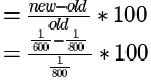
A device with data transfer rate 10 KB/sec is connected to a CPU. Data is transferred byte- wise. Let the interrupt overhead be 4 μsec. The byte transfer time between the device interface register and CPU or memory is negligible. What is the minimum performance gain of operating the device under interrupt mode over operating it under program controlled mode?
a)
15
b)
25
c)
35
d)
45
|
|
Sushant Nambiar answered |

The most appropriate matching for the following pairs
X: Indirect addressing 1: Loops
Y: Immediate addressing 2: Pointers
Z: Auto decrement addressing 3: Constantsis- a)X - 3 Y - 2 Z - 1
- b)X - 1 Y - 3 Z - 2
- c)X - 2 Y - 3 Z - 1
- d)X - 3 Y - 1 Z - 2
Correct answer is option 'C'. Can you explain this answer?
The most appropriate matching for the following pairs
X: Indirect addressing 1: Loops
Y: Immediate addressing 2: Pointers
Z: Auto decrement addressing 3: Constantsis
X: Indirect addressing 1: Loops
Y: Immediate addressing 2: Pointers
Z: Auto decrement addressing 3: Constantsis
a)
X - 3 Y - 2 Z - 1
b)
X - 1 Y - 3 Z - 2
c)
X - 2 Y - 3 Z - 1
d)
X - 3 Y - 1 Z - 2
|
|
Rashi Singh answered |
Explanation:
To determine the correct matching for the given pairs, let's understand the concepts of indirect addressing, immediate addressing, and auto decrement addressing.
Indirect Addressing:
In indirect addressing, the address of the operand is specified by a register or a memory location. It involves accessing the operand indirectly through an intermediate address. It is commonly used for accessing data structures like arrays and linked lists.
Immediate Addressing:
In immediate addressing, the operand itself is specified in the instruction. It means that the data to be operated on is directly given as a constant value in the instruction itself.
Auto Decrement Addressing:
In auto decrement addressing, the address of the operand is decremented automatically after each access. It is often used in stack operations where the top of the stack pointer is decremented after each pop operation.
Now, let's match the given pairs with their corresponding addressing modes:
X: Indirect addressing
Indirect addressing involves accessing the operand indirectly through an intermediate address. It is similar to accessing data structures like arrays and linked lists. Therefore, X matches with 2: Pointers.
Y: Immediate addressing
Immediate addressing means that the operand itself is specified in the instruction. It is directly given as a constant value in the instruction. Therefore, Y matches with 3: Constants.
Z: Auto decrement addressing
Auto decrement addressing involves automatically decrementing the address of the operand after each access. It is commonly used in stack operations. Therefore, Z matches with 1: Loops.
Correct matching:
X - 2
Y - 3
Z - 1
Therefore, the correct matching for the given pairs is option 'C':
X - 2
Y - 3
Z - 1
Which of the following statements is false with regard to instruction pipelining?- a)The basic goal of instruction pipelining is to achieve a CPI of 1.
- b)Instruction set architectures having simple registry/register addressing modes can be easily pipelined than those having complex addressing modes.
- c)By the use of hardware special features and compiler design techniques, pipeline hazards can be removed.
- d)The basic goal of instruction pipelining is to achieve a CPI of more than 1.
Correct answer is option 'D'. Can you explain this answer?
Which of the following statements is false with regard to instruction pipelining?
a)
The basic goal of instruction pipelining is to achieve a CPI of 1.
b)
Instruction set architectures having simple registry/register addressing modes can be easily pipelined than those having complex addressing modes.
c)
By the use of hardware special features and compiler design techniques, pipeline hazards can be removed.
d)
The basic goal of instruction pipelining is to achieve a CPI of more than 1.
|
|
Kavya Mukherjee answered |
The primary goal of instruction pipelining is to achieve a CPI of 1 but not more than 1.
The two numbers given below are multiplied using the Booth’s algorithm.
Multiplicand: 0101101011101110
Multiplier: 0111011110111101Q. How many additions/Subtractions are required for the multiplication of the above two numbers? - a)6
- b)8
- c)10
- d)12
Correct answer is option 'B'. Can you explain this answer?
The two numbers given below are multiplied using the Booth’s algorithm.
Multiplicand: 0101101011101110
Multiplier: 0111011110111101
Multiplicand: 0101101011101110
Multiplier: 0111011110111101
Q. How many additions/Subtractions are required for the multiplication of the above two numbers?
a)
6
b)
8
c)
10
d)
12
|
|
Yashvi Das answered |
Apply Booth’s algorithm:

4 additions and 4 substractions total 8 operations.
4 additions and 4 substractions total 8 operations.
A 5 stage pipeline is used to overlap all the instructions except the branch instructions. The target of the branch can’t be fetched till the current instruction is completed. What is throughput of the system if 20% of instructions are branch instructions? Ignore the overhead of buffer register. Each stage is having same amount delay. The pipeline clock is 10 ns. Branch penalty is of 4 cycles.- a)55 MIPS
- b)45 MIPS
- c)65 MIPS
- d)None of these
Correct answer is option 'A'. Can you explain this answer?
A 5 stage pipeline is used to overlap all the instructions except the branch instructions. The target of the branch can’t be fetched till the current instruction is completed. What is throughput of the system if 20% of instructions are branch instructions? Ignore the overhead of buffer register. Each stage is having same amount delay. The pipeline clock is 10 ns. Branch penalty is of 4 cycles.
a)
55 MIPS
b)
45 MIPS
c)
65 MIPS
d)
None of these
|
|
Gargi Sarkar answered |
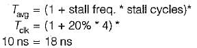
∴ Throughput = Number of instructions executed/ sec
18 ns ........... one instruction
109 ns ......... ?
⇒
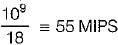
Consider a system with 2 level cache. Access times of Level 1 cache, Level 2 cache and main memory are 1 ns, 10 ns, and500 ns, respectively. The hit rates of Level 1 and Level 2 caches are 0.8 and 0.9, respectively. What is the average accesstime of the system ignoring the search time within the cache?- a)13.0
- b)12.8
- c)12.6
- d)12.4
Correct answer is option 'C'. Can you explain this answer?
Consider a system with 2 level cache. Access times of Level 1 cache, Level 2 cache and main memory are 1 ns, 10 ns, and500 ns, respectively. The hit rates of Level 1 and Level 2 caches are 0.8 and 0.9, respectively. What is the average accesstime of the system ignoring the search time within the cache?
a)
13.0
b)
12.8
c)
12.6
d)
12.4
|
|
Rashi Chakraborty answered |
By default we consider hierarchical access - because that is the common implementation and simultaneous access cache has great practical difficulty. But here the question is a bit ambiguous -- it says to ignore search time within the cache - usually search is applicable for an associative cache but here no such information given. So, may be they are telling to
ignore the search time for L1 and just consider the time for L2 for an L1 miss and similarly just consider memory access time for L2 miss. This is nothing but simultaneous access.
Access time for hierarchical access
ignore the search time for L1 and just consider the time for L2 for an L1 miss and similarly just consider memory access time for L2 miss. This is nothing but simultaneous access.
Access time for hierarchical access


Access time for simultaneous access

 Both options in choice - :O
For interval arithmetic best rounding technique use is ________.- a)Rounding to plus and minus infinity
- b)Rounding to zero
- c)Rounding to nearest
- d)None of these
Correct answer is option 'A'. Can you explain this answer?
For interval arithmetic best rounding technique use is ________.
a)
Rounding to plus and minus infinity
b)
Rounding to zero
c)
Rounding to nearest
d)
None of these
|
|
Diya Chauhan answered |
Rounding to plus and minus infinity are useful in implementing a technique known as interval arithmetic. Interval arithmetic provides an efficient method for monitoring and controlling errors in floating point computations by producing two values for each result. The two values correspond to the lower and upper endpoints of an interval that contains the true result. The width of the interval, which is the difference between the upper and lower endpoints, indicates the accuracy of the result of the endpoints of an interval are not representable then the interval endpoints are rounded down and up respectively.
Microinstruction length is determined by _____.
1. The maximum number of simultaneous micro operations that must be specified.
2. The way in which the control information is represented or encoded.
3. The way in which the next microinstruction address is specified.- a)1 and 2
- b)2 and 3
- c)1 and 3
- d)All of these
Correct answer is option 'D'. Can you explain this answer?
Microinstruction length is determined by _____.
1. The maximum number of simultaneous micro operations that must be specified.
2. The way in which the control information is represented or encoded.
3. The way in which the next microinstruction address is specified.
1. The maximum number of simultaneous micro operations that must be specified.
2. The way in which the control information is represented or encoded.
3. The way in which the next microinstruction address is specified.
a)
1 and 2
b)
2 and 3
c)
1 and 3
d)
All of these
|
|
Maitri Bose answered |
The correct answer is option 'D', which means that all of the given options are factors that determine the microinstruction length. Let's explore each of these factors in detail.
1. The maximum number of simultaneous microoperations that must be specified:
Microinstructions are used to control the operations of a microprogrammed control unit (MCU) within a CPU. These microinstructions typically specify a set of microoperations that need to be executed simultaneously during each machine cycle. The number of microoperations that must be specified in each microinstruction determines the length of the microinstruction. If there are a large number of simultaneous microoperations, the microinstruction length will be longer.
2. The way in which the control information is represented or encoded:
Control information in a microprogrammed control unit is represented using encoding schemes such as binary or one-hot encoding. The choice of encoding scheme affects the number of bits required to represent each control signal. The length of the microinstruction is determined by the total number of bits needed to represent all the control signals. Different encoding schemes may require different lengths of microinstructions.
3. The way in which the next microinstruction address is specified:
Microprograms are typically organized as a sequence of microinstructions stored in a control memory. The next microinstruction to be executed is determined by the address specified in the current microinstruction. The method used to specify the next microinstruction address can vary. It could be a direct address, an indirect address, or an address calculated based on some condition. The way in which the next microinstruction address is specified affects the number of bits required to represent the address, thereby impacting the microinstruction length.
In conclusion, the length of a microinstruction is determined by the maximum number of simultaneous microoperations that must be specified, the encoding scheme used for control information, and the method used to specify the next microinstruction address. All of these factors have an impact on the overall length of the microinstruction.
Consider a Disk I/O transfer, in which 1500 bytes are to be transferred, but number of bytes on a track is 1000, and rotation speed of disk is 1500 rps but the average time required to move the disk arm to the required track is 15 ms, then what will be total access time?- a)16.33 ms
- b)15.33 ms
- c)16.33 μs
- d)15.33 μs
Correct answer is option 'A'. Can you explain this answer?
Consider a Disk I/O transfer, in which 1500 bytes are to be transferred, but number of bytes on a track is 1000, and rotation speed of disk is 1500 rps but the average time required to move the disk arm to the required track is 15 ms, then what will be total access time?
a)
16.33 ms
b)
15.33 ms
c)
16.33 μs
d)
15.33 μs
|
|
Harshitha Sarkar answered |
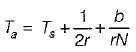
Given:
Ta→ transfer time T
s → average seek time =15 ms
r → rotation speed in rpms = 1500 rps
b → number of bytes to be transferred = 1500 bytes
N → num ber of bytes on a track = 1000 bytes
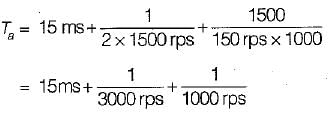
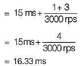
Chapter doubts & questions for Computer Architecture & Organisation (CAO) - GATE Computer Science Engineering(CSE) 2026 Mock Test Series 2025 is part of Computer Science Engineering (CSE) exam preparation. The chapters have been prepared according to the Computer Science Engineering (CSE) exam syllabus. The Chapter doubts & questions, notes, tests & MCQs are made for Computer Science Engineering (CSE) 2025 Exam. Find important definitions, questions, notes, meanings, examples, exercises, MCQs and online tests here.
Chapter doubts & questions of Computer Architecture & Organisation (CAO) - GATE Computer Science Engineering(CSE) 2026 Mock Test Series in English & Hindi are available as part of Computer Science Engineering (CSE) exam.
Download more important topics, notes, lectures and mock test series for Computer Science Engineering (CSE) Exam by signing up for free.
|
© EduRev
|
Education Revolution
|


|


Signup to see your scores
go up
within 7 days!
within 7 days!
Takes less than 10 seconds to signup