All Exams >
GATE Physics >
Electronics for GATE >
All Questions
All questions of P-N Junction Diode for GATE Physics Exam
Calculate form factor of halfwave rectifier as a multiple of π ?
Correct answer is '0.707'. Can you explain this answer?
Calculate form factor of halfwave rectifier as a multiple of π ?
|
|
Chitra Khanna answered |
Understanding Form Factor of Half-Wave Rectifier
The form factor is a crucial parameter in evaluating the performance of a rectifier circuit. It is defined as the ratio of the root mean square (RMS) value of the output voltage to the average value of the output voltage.
Half-Wave Rectifier Basics
- A half-wave rectifier allows only one half of the AC waveform to pass through, blocking the other half.
- It converts AC voltage into pulsating DC voltage.
Calculation of RMS and Average Values
1. Average Output Voltage (V_avg):
- For a half-wave rectifier, the average output voltage can be calculated as:
V_avg = V_m / π
- Here, V_m is the peak voltage of the input AC signal.
2. RMS Output Voltage (V_rms):
- The RMS value for a half-wave rectifier is given by:
V_rms = V_m / 2
Calculating the Form Factor
- The form factor (FF) can be calculated using the formula:
FF = V_rms / V_avg
- Substituting the values:
FF = (V_m / 2) / (V_m / π)
- Simplifying this gives:
FF = π / 2 ≈ 1.57
Conclusion
- The form factor of a half-wave rectifier is approximately 1.57.
- This value indicates the efficiency of the rectification process, helping to evaluate how effectively the AC voltage is converted to DC voltage.
This concise understanding of the form factor provides insight into the performance of half-wave rectifiers.
Which of the following statements is true in case of zener diode?- a)The zener diode is a heavily doped diode
- b)A zener diode is always reverse biased
- c)A zener diode has sharp breakdown voltage
- d)There is no similarity between forward characteristic curve of a diode and zener diode
Correct answer is option 'A,B,C'. Can you explain this answer?
Which of the following statements is true in case of zener diode?
a)
The zener diode is a heavily doped diode
b)
A zener diode is always reverse biased
c)
A zener diode has sharp breakdown voltage
d)
There is no similarity between forward characteristic curve of a diode and zener diode
|
|
Jayant Mishra answered |
We know that zener diode has sharp breakdown voltage. It is always reverse biased and heavily doped diode. There is similarity between forward characteristic curve of a diode.
The correct answers are: A zener diode has sharp breakdown voltage, A zener diode is always reverse biased, The zener diode is a heavily doped diode
The correct answers are: A zener diode has sharp breakdown voltage, A zener diode is always reverse biased, The zener diode is a heavily doped diode
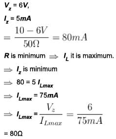
A 24V, 600mW, zener diode is to be used in for providing a 24 Vstabilized supply to variable load.
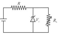
Assuming for a proper zener action, a minimum of 10mA must flow through the zener. If the input voltage is 32 V. What would be the value of RL (in ohm).
Correct answer is '320'. Can you explain this answer?
A 24V, 600mW, zener diode is to be used in for providing a 24 Vstabilized supply to variable load.

Assuming for a proper zener action, a minimum of 10mA must flow through the zener. If the input voltage is 32 V. What would be the value of RL (in ohm).

Assuming for a proper zener action, a minimum of 10mA must flow through the zener. If the input voltage is 32 V. What would be the value of RL (in ohm).

|
Pie Academy answered |


The correct answer is: 320
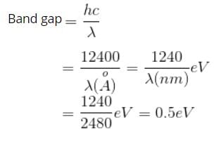
The correct sequence of band gaps of germanium  silicon
 and gallium arsenide
 will :
- a)

- b)

- c)

- d)

Correct answer is option 'C'. Can you explain this answer?
The correct sequence of band gaps of germanium  silicon
 and gallium arsenide
 will :
 silicon
 and gallium arsenide
 will :
a)

b)

c)

d)

|
|
Jayant Mishra answered |
The energy gap of gallium is maximum whereas silicon has less Eg than that of germanium.
The correct answer is:
The correct answer is:

Which graph represents the nature of the curve between charge density p and distance r near the depletion region of p-n junction diode?- a)
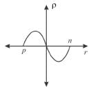
- b)
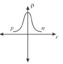
- c)
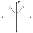
- d)
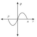
Correct answer is option 'D'. Can you explain this answer?
Which graph represents the nature of the curve between charge density p and distance r near the depletion region of p-n junction diode?
a)

b)

c)

d)

|
|
Vedika Singh answered |
Holes will diffuse to right and electrons to left junction initially. Positive holes neutralize the acceptor ions near the function in the p-type silicon and disappeared across junction. Similarly, electrons will be neutralized across n-type by combination with holes of p-type due to diffusion. Thus, across p-type and n-type, there will be lack of majority charge carriers and excess of minority charge carriers. Then, majority charge carriers decreases as we move away from junction.
The Correct answer is
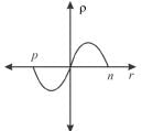
The Correct answer is

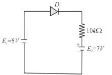
What is the diode current (A) in the circuit:
Correct answer is '0'. Can you explain this answer?
What is the diode current (A) in the circuit:


|
|
Vedika Singh answered |
Diode will be in conducting state, when forward biased voltage is applied to it and in non-conducting state, when reverse biased voltage is applied to it. Now, the two batteries may be replaced by a single battery of 2Vwhich will make the diode reverse biased and diode goes to non-conducting state and hence current is zero
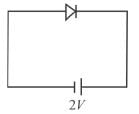
The correct answer is: 0

The correct answer is: 0
pure silicon at 300K has equal electrons concentrations (ne) and hole concentration (nh) of 1.5 x 10¹⁶ m-3 . Doping by sodium increases nh to 4.5 x 10²² m-3 . Then ne in the doped silicon is :- a)

- b)

- c)

- d)

Correct answer is option 'B'. Can you explain this answer?
pure silicon at 300K has equal electrons concentrations (ne) and hole concentration (nh) of 1.5 x 10¹⁶ m-3 . Doping by sodium increases nh to 4.5 x 10²² m-3 . Then ne in the doped silicon is :
a)

b)

c)

d)


|
Pie Academy answered |
Under thermal equilibrium, the product of free electron concentration n and hole 9 e concentration nh is constant equal to  where ni is the concentration of intrinsic semiconductor
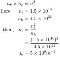
The correct answer is:

 where ni is the concentration of intrinsic semiconductor
The correct answer is:

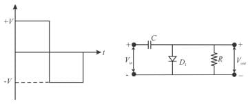
For the clamping network shown below, the resulting output for the applied input will be.
- a)

- b)
- c)
- d)
Correct answer is option 'A'. Can you explain this answer?
For the clamping network shown below, the resulting output for the applied input will be.


a)

b)

c)

d)

|
|
Vedika Singh answered |
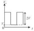
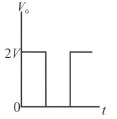
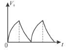
For the first position half of the input signal, the current pass through the diode, hence no current flows through the resistor R, hence, no output voltage is observed and capacitor is charged upto voltage V. For second half (negative), diode blocks the flow of current, hence current pass through resistor R but in opposite direction, hence the potential difference observed across R comes input from signal-V and from the capacitor again in opposite direction, thus making it-2V.
The correct answer is:
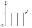
The correct answer is:

If the barrier potential change with biasing of a p-n junction diode, then the barrier potential will.- a)increase with reverse bias
- b)decrease with reverse bias
- c)increase with forward bias
- d)decrease with forward bias
Correct answer is option 'A,D'. Can you explain this answer?
If the barrier potential change with biasing of a p-n junction diode, then the barrier potential will.
a)
increase with reverse bias
b)
decrease with reverse bias
c)
increase with forward bias
d)
decrease with forward bias
|
|
Jayant Mishra answered |
For a p-n junction diode, barrier potential decreases with forward and increases with reverse biasing.
The correct answers are: increase with reverse bias, decrease with forward bias
The correct answers are: increase with reverse bias, decrease with forward bias
The fermi level of an intrinsic semi-conductor is pinned at the centre of the band-gap. The probability of occupation of the highest electronic state in valence band at room temperature, will b e :- a)between zero and half
- b)one
- c)half
- d)zero
Correct answer is option 'C'. Can you explain this answer?
The fermi level of an intrinsic semi-conductor is pinned at the centre of the band-gap. The probability of occupation of the highest electronic state in valence band at room temperature, will b e :
a)
between zero and half
b)
one
c)
half
d)
zero
|
|
Vedika Singh answered |
According to Fermi-Dirac distribution law, the probability of an electron in finding energy level E at temperature T is given as


By (i) and (ii),

The correct answer is: half


By (i) and (ii),

The correct answer is: half
A p-n diode is reverse biased. The resistance measured by an ohm-meter connected across it will be.
- a)infinity
- b)zero
- c)high
- d)low
Correct answer is option 'C'. Can you explain this answer?
A p-n diode is reverse biased. The resistance measured by an ohm-meter connected across it will be.
a)
infinity
b)
zero
c)
high
d)
low
|
|
Jayant Mishra answered |
In case of reverse biased, the resistance of an ideal p-n diode should be infinity. But practically infinite is not possible and so resistance becomes very high.
The correct answer is: high
The correct answer is: high
A 10V zener diode working as a voltage regulator operates from a source that varies from 5 V to 15V, the series resistance is 0.1kΩ and the load draws a current that varies from 0 to 20mA. The power dissipation in the zener diode under worst case (in Watts) is?
Correct answer is '0.5'. Can you explain this answer?
A 10V zener diode working as a voltage regulator operates from a source that varies from 5 V to 15V, the series resistance is 0.1kΩ and the load draws a current that varies from 0 to 20mA. The power dissipation in the zener diode under worst case (in Watts) is?
|
|
Vedika Singh answered |
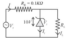
For maximum power dissipation, current through zener diode should be maximum which is maximum when total current in the circuit is maximum i.e. Vs = 15V.

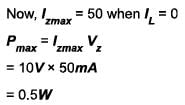
The correct answer is: 0.5
When reverse voltage across silicon diode is changed from 4V to 8 V, what happens to depletion layer?- a)It may increase or decrease
- b)It is unaffected
- c)It increases
- d)It decreases
Correct answer is option 'D'. Can you explain this answer?
When reverse voltage across silicon diode is changed from 4V to 8 V, what happens to depletion layer?
a)
It may increase or decrease
b)
It is unaffected
c)
It increases
d)
It decreases
|
|
Jayant Mishra answered |
When reverse voltage is applied across the silicon diode. If its voltage is increased, then its depletion layer be decreased.
The correct answer is: It decreases
The correct answer is: It decreases
Consider the following statements regarding the magnitude of barrier potential of a p- n junction. Which of them are true?- a)It depends on difference between fermi levels on two sides of fermi level
- b)It depends on impurity concentration in p and n-type semiconductors
- c)It depends on forbidden energy-gap on two types of semiconductors
- d)It is independent of temperature
Correct answer is option 'A,B,C'. Can you explain this answer?
Consider the following statements regarding the magnitude of barrier potential of a p- n junction. Which of them are true?
a)
It depends on difference between fermi levels on two sides of fermi level
b)
It depends on impurity concentration in p and n-type semiconductors
c)
It depends on forbidden energy-gap on two types of semiconductors
d)
It is independent of temperature
|
|
Jayant Mishra answered |
When a p-type semiconductor having holes as majority carrier is clamped with a ntype semiconductor having electron as majority carrier.
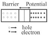
Some electrons from n-side goes to p-side and some holes goes to n-side, thus creates a potential barrier, which
(i) depends on temperature
(ii) depends on fermi level
(iii) forbidden energy gap Eg
(iv) majority carriers
The correct answers are: It depends on difference between fermi levels on two sides of fermi level, It depends on forbidden energy-gap on two types of semiconductors, It depends on impurity concentration in p and n-type semiconductors
What is the maximum electric field when Vbi = 2V, VR = 5V and width of the semiconductor is 7cm? - a)-100V/m
- b)100V/m
- c)200V/m
- d)-200V/m
Correct answer is option 'D'. Can you explain this answer?
What is the maximum electric field when Vbi = 2V, VR = 5V and width of the semiconductor is 7cm?
a)
-100V/m
b)
100V/m
c)
200V/m
d)
-200V/m
|
|
Vedika Singh answered |
Emax = -2(Vbi + VR) / W
= -2(2 + 5) / (7 * 10-2)
= -200V/m.
= -2(2 + 5) / (7 * 10-2)
= -200V/m.
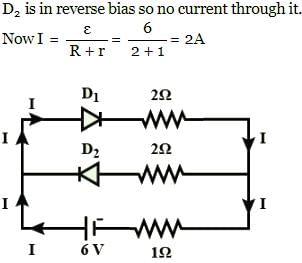
What is the potential difference across R1 (in volts) ?
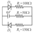
Correct answer is '2'. Can you explain this answer?
What is the potential difference across R1 (in volts) ?


|
|
Jayant Mishra answered |
D2 is reverse biased, hence, no current flow through it.
6 - iR2 - iR1=0

Now potential difference across R1
= 2V
The correct answer is: 2
6 - iR2 - iR1=0

Now potential difference across R1

= 2V
The correct answer is: 2
An avalanche effect is observed in a diode when- a)the forward voltage is less than the breakdown voltage
- b)the reverse voltage exceeds the breakdown voltage
- c)the diode is heavily doped and forward biassed
- d)the forward voltage exceeds the breakdown voltage X
Correct answer is option 'B'. Can you explain this answer?
An avalanche effect is observed in a diode when
a)
the forward voltage is less than the breakdown voltage
b)
the reverse voltage exceeds the breakdown voltage
c)
the diode is heavily doped and forward biassed
d)
the forward voltage exceeds the breakdown voltage X
|
|
Jayant Mishra answered |
The avalanche effect is observed when reverse biased voltage is more than the breakdown voltage.
The correct answer is: the reverse voltage exceeds the breakdown voltage
The correct answer is: the reverse voltage exceeds the breakdown voltage
An ac voltage of 220 Vrms is applied to the primary of a 10:1 step-down transformer. The secondary of the transformer is centre tapped and connected to a full-wave rectifier with a load resistance. This dc voltage appearing in the load is.- a)44/π
- b)31/π
- c)62/π
- d)22/π
Correct answer is option 'A'. Can you explain this answer?
An ac voltage of 220 Vrms is applied to the primary of a 10:1 step-down transformer. The secondary of the transformer is centre tapped and connected to a full-wave rectifier with a load resistance. This dc voltage appearing in the load is.
a)
44/π
b)
31/π
c)
62/π
d)
22/π
|
|
Vedika Singh answered |
For step-down transformer,
E < E1
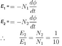
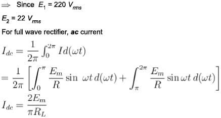
(44/π)
E < E1


(44/π)
A sinusoidal input voltage Vin of frequency ω is fed to the circuit shown in the figure where  if Vm the Peak value of the input voltage, then output voltage (Vout) is.

- a)

- b)

- c)

- d)

Correct answer is option 'D'. Can you explain this answer?
A sinusoidal input voltage Vin of frequency ω is fed to the circuit shown in the figure where  if Vm the Peak value of the input voltage, then output voltage (Vout) is.

 if Vm the Peak value of the input voltage, then output voltage (Vout) is.
a)

b)

c)

d)


|
Pie Academy answered |
The circuit looks like a voltage doubler. At the peak of positive half cycle D1 is forward biased and D2 is reverse biased. Ideally, this charges C1 to the peak voltage Vm , with polarity as shown below. At the peak of the negative half cycle, D1 is reverse biased and D2 is forward biased. Because the source and C1 are in series, C2 will try to change towards 2Vm
The correct answer is:
The correct answer is:

Which of the following electronic devices are used to make a clamper?- a)Resistor
- b)Diode
- c)Capacitor
- d)Inductor
Correct answer is option 'A,B,C'. Can you explain this answer?
Which of the following electronic devices are used to make a clamper?
a)
Resistor
b)
Diode
c)
Capacitor
d)
Inductor

|
Pie Academy answered |
A normal clamper consists of a diode, a resistor and a capacitor that shifts a waveform to a different dc level without changing the appearance of the applied signal.
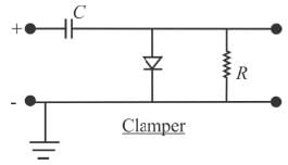
The correct answers are: Capacitor, Diode, Resistor

The correct answers are: Capacitor, Diode, Resistor
Current 2A and 1A flow when large forward voltage V1 and V2 are applied to a semiconductor diode. If V1, = V2, then the value of the reverse saturation current is. (in A)
Correct answer is '0.5'. Can you explain this answer?
Current 2A and 1A flow when large forward voltage V1 and V2 are applied to a semiconductor diode. If V1, = V2, then the value of the reverse saturation current is. (in A)
|
|
Jaidev Reddy answered |
Explanation:
When a large forward voltage V1 and V2 are applied to a semiconductor diode, the diode is said to be forward biased. In this case, the current flows easily through the diode, and it is called the forward current.
Forward Current:
- The forward current in a diode is primarily carried by majority charge carriers (electrons in N-type and holes in P-type).
- The current is directly proportional to the forward voltage applied to the diode.
- The relationship between forward voltage and forward current is given by the diode equation: I = Is * (e^(Vf / Vt) - 1), where I is the forward current, Is is the reverse saturation current, Vf is the forward voltage, and Vt is the thermal voltage (approximately 0.026 V at room temperature).
Reverse Saturation Current:
- The reverse saturation current (Is) is the current that flows through a diode when it is reverse biased and a large reverse voltage is applied.
- In an ideal diode, the reverse saturation current is assumed to be negligible (close to zero).
- However, in practical diodes, there is always a small amount of reverse current that flows due to minority charge carriers and other factors.
- The value of the reverse saturation current is typically very small, on the order of microamperes (10^-6 A) or even smaller.
Given Conditions:
- V1 = V2 (large forward voltage applied to the diode)
- The value of the reverse saturation current is to be determined.
Solution:
- Since V1 = V2, it implies that both diodes are forward biased with the same voltage.
- Therefore, the forward current flowing through each diode will be the same.
- Using the diode equation, we can write: I1 = I2 = Is * (e^(Vf / Vt) - 1)
- Since the forward currents are the same, we can equate the equations for I1 and I2:
Is * (e^(Vf / Vt) - 1) = Is * (e^(Vf / Vt) - 1)
- Canceling out the common terms on both sides, we get:
e^(Vf / Vt) - 1 = e^(Vf / Vt) - 1
- This equation is satisfied for any value of the reverse saturation current (Is).
- Therefore, the value of the reverse saturation current can be any non-zero value, including 0.5 A.
Conclusion:
- The value of the reverse saturation current is not uniquely determined by the given conditions.
- It can be any non-zero value, including 0.5 A.
If a zener diode (Vz = 5V and lz = 10 mA) is connected in series with a resistance and 20V is applied across the combination, then the maximum resistance one can use without spoiling zener action (in kΩ) is :
Correct answer is '1.5'. Can you explain this answer?
If a zener diode (Vz = 5V and lz = 10 mA) is connected in series with a resistance and 20V is applied across the combination, then the maximum resistance one can use without spoiling zener action (in kΩ) is :
|
|
Jayant Mishra answered |
The principal use of a zener diode is in a voltage regulator. In a voltage regulator, the voltage across the load remains constant over a range of current.
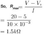
The correct answer is: 1.5

The correct answer is: 1.5
A silicon diode is in series with a 1.0kΩ resistor and a 5V battery. If the node is connected to the positive battery terminal, the cathode voltage with respect to the negative battery terminal is (in Volts)
Correct answer is '4.3'. Can you explain this answer?
A silicon diode is in series with a 1.0kΩ resistor and a 5V battery. If the node is connected to the positive battery terminal, the cathode voltage with respect to the negative battery terminal is (in Volts)
|
|
Vedika Singh answered |
The cathode voltage with respect to the negative battery terminal is
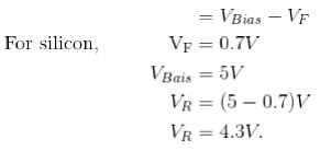
The correct answer is: 4.3

The correct answer is: 4.3
When three zener diodes of identical specification having 10W, 10 V, l000 mA are connected in series to a 45V~dc power supply. Calculate the series resistance required to obtain 30 V regulated output (in Ω)?
Correct answer is '15'. Can you explain this answer?
When three zener diodes of identical specification having 10W, 10 V, l000 mA are connected in series to a 45V~dc power supply. Calculate the series resistance required to obtain 30 V regulated output (in Ω)?
|
|
Vedika Singh answered |
Power of each diode = 10W
Potential = 10V
⇒ current = 1A
⇒ Resistance of each zener diode R
⇒ Equivalent resistance of three diodes connected in series
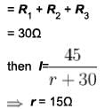
The correct answer is: 15
Potential = 10V
⇒ current = 1A
⇒ Resistance of each zener diode R

⇒ Equivalent resistance of three diodes connected in series

The correct answer is: 15
For a zener diode, Vz = 20 V and power rating of 0.2W. If the source battery provides a potential difference of 50 V. The minimum value of Rs in Ω that prevents zener diode from being destroyed is.
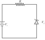
Correct answer is '3000'. Can you explain this answer?
For a zener diode, Vz = 20 V and power rating of 0.2W. If the source battery provides a potential difference of 50 V. The minimum value of Rs in Ω that prevents zener diode from being destroyed is.


|
Pie Academy answered |
Maximum zener current

Minimum value of Rs=


The correct answer is: 3000

Minimum value of Rs=


The correct answer is: 3000
For an intrinsic semiconductor,  are respectively, the effective masses of electrons and holes near the corresponding band edges. At a finite temperature, the position of fermi level:
- a)depends on
 but not on
- b)depends on

- c)depends on
 but not on
- d)depends on

Correct answer is option 'B,D'. Can you explain this answer?
For an intrinsic semiconductor,  are respectively, the effective masses of electrons and holes near the corresponding band edges. At a finite temperature, the position of fermi level:
 are respectively, the effective masses of electrons and holes near the corresponding band edges. At a finite temperature, the position of fermi level:
a)
depends on but not on
 but not on
b)
depends on

c)
depends on but not on
 but not on
d)
depends on

|
|
Jayant Mishra answered |
The finite temperature, the position of fermi level would depend on both 
The correct answers are: depends on , depends on

The correct answers are: depends on
 , depends on
The voltage across a diode in a full-wave rectifier having input voltage of peak value Vm during its non-conducting period is :- a)-2Vm
- b)-Vm
- c)-4Vm
- d)0
Correct answer is option 'A'. Can you explain this answer?
The voltage across a diode in a full-wave rectifier having input voltage of peak value Vm during its non-conducting period is :
a)
-2Vm
b)
-Vm
c)
-4Vm
d)
0
|
|
Vedika Singh answered |
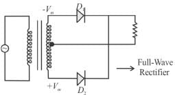
During non-conducting period, the voltage across D1 is Vm. = -2Vm.
The correct answer is:

A zener diode is also a p-n junction diode. It can be used as :- a)half-wave rectifier
- b)ac voltage regulator
- c)full wave-rectifier
- d)dc voltage regulator X
Correct answer is option 'C'. Can you explain this answer?
A zener diode is also a p-n junction diode. It can be used as :
a)
half-wave rectifier
b)
ac voltage regulator
c)
full wave-rectifier
d)
dc voltage regulator X
|
|
Jayant Mishra answered |
A zener diode can be used as full-wave rectifier. The electronic instrument which converts ac into dc is known as rectifier.
The correct answer is: full wave-rectifier
The correct answer is: full wave-rectifier
An ideal switch is one which has :- a)Zero resistance when OFF
- b)Zero resistance when ON
- c)Infinite resistance when OFF
- d)Infinite resistance when ON
Correct answer is option 'B,C'. Can you explain this answer?
An ideal switch is one which has :
a)
Zero resistance when OFF
b)
Zero resistance when ON
c)
Infinite resistance when OFF
d)
Infinite resistance when ON
|
|
Jayant Mishra answered |
Characteristics of any ideal switch is that it should offer zero resistance when ON and infinite resistance when OFF.
The correct answers are: Zero resistance when ON, Infinite resistance when OFF
The correct answers are: Zero resistance when ON, Infinite resistance when OFF
If RL = 1kΩ, find the maximum zener current (in mA).
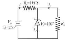
Correct answer is '5'. Can you explain this answer?
If RL = 1kΩ, find the maximum zener current (in mA).


|
|
Jayant Mishra answered |

Voltage developed across
 always.
For maximum current l (and hence also zener current lz),Vin = 25V.
Applying KVL across loop 1, we have
(25 -10 ) = 10 x 103 x l

Hence, maximum zener current.
lz = (15 - 10)
= 5mA
The correct answer is: 5
The centre tap full-wave single phase rectifier circuit uses 2 diodes as shown in the given figure. The rms voltage across each diode is (in Volts)
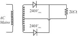
Correct answer is '339.4'. Can you explain this answer?
The centre tap full-wave single phase rectifier circuit uses 2 diodes as shown in the given figure. The rms voltage across each diode is (in Volts)


|
Pie Academy answered |
Peak inverse voltage (PIV) across each diode = when diode is conducting (during half cycle) the voltage across the diode is zero.
Hence, rms value of voltage across the diode =
The correct answer is: 339.4
 when diode is conducting (during half cycle) the voltage across the diode is zero.
Hence, rms value of voltage across the diode =

The correct answer is: 339.4
Which of the following devices is forward bias in its normal mode of operation.- a)Solar cell
- b)Zener diode
- c)Avalanche photodiode
- d)LASER diode
Correct answer is option 'A,D'. Can you explain this answer?
Which of the following devices is forward bias in its normal mode of operation.
a)
Solar cell
b)
Zener diode
c)
Avalanche photodiode
d)
LASER diode
|
|
Hamsini Rana answered |
Forward Bias in Devices:
Forward bias is a condition in which the positive terminal of a voltage source is connected to the p-region of a diode, and the negative terminal is connected to the n-region. This forward biasing allows current to flow through the diode, enabling it to operate in its normal mode.
Solar Cell:
A solar cell is a device that converts sunlight directly into electricity. When sunlight strikes the solar cell, it generates electron-hole pairs, creating a voltage across the p-n junction. The solar cell is typically connected in a forward bias configuration, allowing the generated current to flow through an external circuit.
Laser Diode:
A laser diode is a semiconductor device that emits coherent light through stimulated emission. To operate, a laser diode is typically forward biased. The forward bias voltage provides the necessary energy for the stimulated emission process to occur, resulting in the emission of laser light.
Zener Diode:
A Zener diode is a special type of diode that operates in the reverse breakdown region. It is primarily used for voltage regulation. While a Zener diode can be operated in a forward bias mode, its normal mode of operation is in reverse bias, where it exhibits a controlled breakdown voltage.
Avalanche Photodiode:
An avalanche photodiode is a highly sensitive semiconductor device used to detect light. It operates in the reverse bias mode, where the reverse voltage applied across the diode creates an internal electric field. When photons strike the diode, they generate electron-hole pairs, which are then multiplied through an avalanche process. This multiplication is achieved by the high electric field, allowing for high sensitivity in detecting light.
Conclusion:
Based on the given options, the devices that are forward biased in their normal mode of operation are the solar cell and laser diode. The solar cell operates in a forward bias mode to convert sunlight into electricity, while the laser diode requires forward biasing to emit laser light. On the other hand, the Zener diode operates in reverse bias for voltage regulation, and the avalanche photodiode operates in reverse bias for light detection.
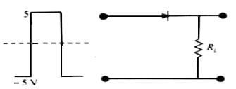
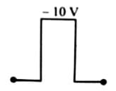
If in a p-n junction diode, a square input signal of 8V is applied (see figure below), what is the value of output signal across RL?
- a)
- b)

- c)

- d)

Correct answer is option 'C'. Can you explain this answer?
If in a p-n junction diode, a square input signal of 8V is applied (see figure below), what is the value of output signal across RL?


a)

b)

c)

d)

|
|
Jayant Mishra answered |

When the voltage is −5 V, the diode will be reverse biased and the voltage drop across the resistor will be zero as there is no current in the circuit. And when voltage is +5 V, the diode will be forward biased, the voltage drop across resistor will be thAe same as input voltage.
The depletion layers in a p-n junction diode consists of layers of :- a)Negatively charged on the p-side and positively charged acceptors on the n- side
- b)Positively charged donors on the p-side and negatively charged acceptors on the /7-side
- c)Positively charged donors on the n-side and negatively charged acceptors on the p-side
- d)Negatively charged donors on the n-side and positively charged acceptors on the p-side
Correct answer is option 'C'. Can you explain this answer?
The depletion layers in a p-n junction diode consists of layers of :
a)
Negatively charged on the p-side and positively charged acceptors on the n- side
b)
Positively charged donors on the p-side and negatively charged acceptors on the /7-side
c)
Positively charged donors on the n-side and negatively charged acceptors on the p-side
d)
Negatively charged donors on the n-side and positively charged acceptors on the p-side
|
|
Jayant Mishra answered |
The depletion layer in p-n junction consists of the layer of positively charged donors on the n-side and negatively charged acceptors on p-side.

The correct answer is: Positively charged donors on the n-side and negatively charged acceptors on the p-side

The correct answer is: Positively charged donors on the n-side and negatively charged acceptors on the p-side
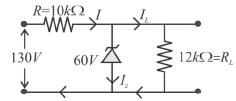
Calculate the zener current in the given circuit in mA?
Correct answer is '2'. Can you explain this answer?
Calculate the zener current in the given circuit in mA?


|
Pie Academy answered |

and

Now 130-60 = IR

Now, Vz = lLRL

Iz = 2mA
The correct answer is: 2
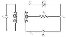
For the rectifier circuit shown in figure, the sinusoidal voltage (V1 or V2) at the output transformer has a maximum value of 10 V. The load resistance RL is 1kΩ. What is the value of lav as a multiple of 
Correct answer is '20'. Can you explain this answer?
For the rectifier circuit shown in figure, the sinusoidal voltage (V1 or V2) at the output transformer has a maximum value of 10 V. The load resistance RL is 1kΩ. What is the value of lav as a multiple of 


|
|
Vedika Singh answered |
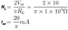
The correct answer is: 20
When two identical zener diodes are connected in series, what happens to the breakdown voltage of the combination ?- a)It remains same
- b)It becomes zero)
- c)It is halved
- d)It is doubled
Correct answer is option 'C'. Can you explain this answer?
When two identical zener diodes are connected in series, what happens to the breakdown voltage of the combination ?
a)
It remains same
b)
It becomes zero)
c)
It is halved
d)
It is doubled
|
|
Jayant Mishra answered |
Since, two diodes are connected in series, the breakdown voltage of combination becomes almost double than that of a single diode.
The correct answer is: It is halved
The correct answer is: It is halved
A half-wave rectifier employs a transformer with turn ratio n1 : n2 = 12 : 1. If primary coil is connected to the power mains 220V, 50Hz. If the diode resistance in forward bias is negligible, what is the peak inverse voltage (in Volts) of the diode?
Correct answer is '25 .9'. Can you explain this answer?
A half-wave rectifier employs a transformer with turn ratio n1 : n2 = 12 : 1. If primary coil is connected to the power mains 220V, 50Hz. If the diode resistance in forward bias is negligible, what is the peak inverse voltage (in Volts) of the diode?
|
|
Vedika Singh answered |
The turn ratio of transform ation is 12:1. So if primary coil is connected to power mains o f 220V , then potential of secondary coil is  Volts. In a half-wave rectifier,
 is the maximum voltage appearing across the transformer secondary coil. Now. peak inverse voltage,
  for half wave rectifier in given as V0

= 25.9V
The correct answer is: 25 .9
 Volts. In a half-wave rectifier,
 is the maximum voltage appearing across the transformer secondary coil. Now. peak inverse voltage,
  for half wave rectifier in given as V0
= 25.9V
The correct answer is: 25 .9
Calculate the diffusion current density when the concentration of electron varies from the 1 * 1018 to 7 * 1017 cm-3 over a distance of 0.10 cm. D = 225cm2/s
Correct answer is '108A/cm2'. Can you explain this answer?
Calculate the diffusion current density when the concentration of electron varies from the 1 * 1018 to 7 * 1017 cm-3 over a distance of 0.10 cm. D = 225cm2/s
|
|
Vedika Singh answered |
J = eDdn / dx
J = 1.6 * 10-19 * 225 * (1018 - (7 * 1017)) / 0.1
= 108A/cm2.
J = 1.6 * 10-19 * 225 * (1018 - (7 * 1017)) / 0.1
= 108A/cm2.
For a full wave rectifier:- a)We need two diodes placed at opposite polarity
- b)Maximum Rectification efficiency η= 81.1 %
- c)Average value of load current is

- d)Ripple factor = 0.483
Correct answer is option 'A,B,D'. Can you explain this answer?
For a full wave rectifier:
a)
We need two diodes placed at opposite polarity
b)
Maximum Rectification efficiency η= 81.1 %
c)
Average value of load current is 

d)
Ripple factor = 0.483
|
|
Jayant Mishra answered |
Full wave rectifier consists of two diodes each with different polarity ends which help it keep running both in positive and negative half. Average or dc value of load current 
The correct answers are: We need two diodes placed at opposite polarity, Ripple factor = 0.483, Maximum Rectification efficiency η = 81.1 %

The correct answers are: We need two diodes placed at opposite polarity, Ripple factor = 0.483, Maximum Rectification efficiency η = 81.1 %
A 60 V peak full wave rectified voltage is applied to a capacitor input filter. If f = 120Hz, RL=10Ω and C=10μF, the ripple voltage (V) is :
Correct answer is '5'. Can you explain this answer?
A 60 V peak full wave rectified voltage is applied to a capacitor input filter. If f = 120Hz, RL=10Ω and C=10μF, the ripple voltage (V) is :
|
|
Vedika Singh answered |
Peak to peak ripple voltage for capacitor input filter,
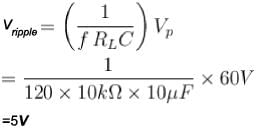
The correct answer is: 5

The correct answer is: 5
Which of the following statements are true for a clamper?- a)consists of capacitor and inductor
- b)does not change appearance of input signal
- c)changes the appearance of input signal
- d)shifts dc level of the waveform
Correct answer is option 'B,D'. Can you explain this answer?
Which of the following statements are true for a clamper?
a)
consists of capacitor and inductor
b)
does not change appearance of input signal
c)
changes the appearance of input signal
d)
shifts dc level of the waveform
|
|
Hamsini Rana answered |
Introduction:
A clamper is a circuit that is used to shift the DC level of a waveform without changing its shape or altering the frequency content. It consists of a capacitor and a diode, and it can be used to add or remove a DC offset from a signal.
Explanation:
b) Does not change the appearance of the input signal:
A clamper circuit does not change the shape or frequency content of the input signal. It only shifts the DC level of the waveform. The AC component of the input signal remains unchanged.
When an input signal is applied to a clamper circuit, the capacitor charges or discharges through the diode, depending on the polarity of the input signal. This charging or discharging process causes a shift in the DC level of the waveform.
d) Shifts the DC level of the waveform:
The main purpose of a clamper circuit is to shift the DC level of a waveform. This means that the entire waveform is shifted either upwards or downwards by a certain amount. The AC component of the waveform remains unaffected.
The amount of DC shift depends on the charging or discharging time constant of the capacitor. If the capacitor charges slowly, the DC level of the waveform will shift upwards. On the other hand, if the capacitor discharges slowly, the DC level will shift downwards.
Example:
Let's consider an example to understand the operation of a clamper circuit. Suppose we have an input signal with a DC offset of +2V and an amplitude of 2V. When this signal is applied to a clamper circuit with a positive clamper configuration, the diode conducts during the positive half-cycle of the input signal.
During the positive half-cycle, the capacitor charges through the diode, resulting in a shift in the DC level of the waveform. If the charging time constant is chosen appropriately, the DC level can be shifted to a desired value. In this case, the DC level will be shifted to +2V + the charge on the capacitor.
During the negative half-cycle, the diode is reverse biased and does not conduct. Therefore, the capacitor remains charged at the desired level, and the waveform appears shifted.
Conclusion:
In conclusion, a clamper circuit consists of a capacitor and a diode. It does not change the appearance or frequency content of the input signal but only shifts the DC level of the waveform. This makes it useful for adding or removing a DC offset from a signal without altering its shape.
The built-in potential of p-n junction diode is a function of.- a)Temperature
- b)Biased voltage
- c)Doping density
- d)None of the above
Correct answer is option 'A,B,C'. Can you explain this answer?
The built-in potential of p-n junction diode is a function of.
a)
Temperature
b)
Biased voltage
c)
Doping density
d)
None of the above

|
Pie Academy answered |
Formation of potential of p-n junction diode depends on temperature, biased voltage and doping density.
The correct answers are: Temperature, Biased voltage, Doping density
The correct answers are: Temperature, Biased voltage, Doping density
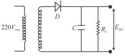
The below figure shows a half-wave rectifier with resistive load RL, which is far greater than the diode forward resistance. If the value of capacitor C is considerably large, then the dc voltage across RL is :
- a)5V
- b)14V
- c)28V
- d)10V
Correct answer is option 'A'. Can you explain this answer?
The below figure shows a half-wave rectifier with resistive load RL, which is far greater than the diode forward resistance. If the value of capacitor C is considerably large, then the dc voltage across RL is :


a)
5V
b)
14V
c)
28V
d)
10V
|
|
Vedika Singh answered |
For half-wave rectifier, the current in load is given as

and voltage

= 5V
The correct answer is: 5V

and voltage

= 5V
The correct answer is: 5V
Chapter doubts & questions for P-N Junction Diode - Electronics for GATE 2025 is part of GATE Physics exam preparation. The chapters have been prepared according to the GATE Physics exam syllabus. The Chapter doubts & questions, notes, tests & MCQs are made for GATE Physics 2025 Exam. Find important definitions, questions, notes, meanings, examples, exercises, MCQs and online tests here.
Chapter doubts & questions of P-N Junction Diode - Electronics for GATE in English & Hindi are available as part of GATE Physics exam.
Download more important topics, notes, lectures and mock test series for GATE Physics Exam by signing up for free.
Electronics for GATE
55 videos|28 docs|20 tests
|

Contact Support
Our team is online on weekdays between 10 AM - 7 PM
Typical reply within 3 hours
|
Free Exam Preparation
at your Fingertips!
Access Free Study Material - Test Series, Structured Courses, Free Videos & Study Notes and Prepare for Your Exam With Ease

 Join the 10M+ students on EduRev
|

|
Create your account for free
OR
Forgot Password
OR
Signup to see your scores
go up
within 7 days!
within 7 days!
Takes less than 10 seconds to signup
