


Electrical Engineering (EE) Exam > Electrical Engineering (EE) Questions > A FET tuned amplifier with gm = 5 mA/V, rd = ...
Start Learning for Free
A FET tuned amplifier with gm = 5 mA/V, rd = 20 kΩ has a resonant impedance of 20 kΩ. The gain at resonance is given by
- a)200
- b)100
- c)50
- d)25
Correct answer is option 'C'. Can you explain this answer?

Verified Answer
A FET tuned amplifier with gm = 5 mA/V, rd = 20 kΩhas a resonant...
AV = Gain at resonance = gmR
Here, R = rd ║Rmax
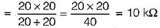
∴ AV = 5x 10-3 x 10 x 103 = 50
Here, R = rd ║Rmax
∴ AV = 5x 10-3 x 10 x 103 = 50
Most Upvoted Answer
A FET tuned amplifier with gm = 5 mA/V, rd = 20 kΩhas a resonant...
A FET tuned amplifier refers to an amplifier circuit that uses a field-effect transistor (FET) as the active device and is designed to amplify a specific frequency range.
Given the parameters:
- gm = 5 mA/V: This represents the transconductance of the FET, which is a measure of how much the drain current changes with respect to the gate-source voltage. In this case, the transconductance is 5 mA per volt.
- rd = 20 kΩ: This represents the drain-source resistance of the FET, which is also known as the output impedance. It is the resistance seen looking into the drain terminal with the source terminal shorted to ground.
To design a FET tuned amplifier, you would typically need additional information such as the desired frequency range, the gain requirements, input/output impedance requirements, etc. However, I can provide a general overview of the circuit.
A common configuration for a FET tuned amplifier is the common-source configuration, which provides high voltage gain and good input/output isolation. The key components in this configuration include:
1. FET: The FET is the active device that provides amplification. In this case, the FET has a transconductance of 5 mA/V and an output impedance of 20 kΩ.
2. Biasing Network: The FET requires proper biasing to operate in the active region. This typically involves using resistors and/or capacitors to provide the appropriate DC bias voltage at the gate and drain terminals.
3. Tuning Network: The tuning network consists of inductors and capacitors that are used to select the desired frequency range for amplification. These components create a resonant circuit that provides a narrow bandwidth around the desired frequency.
4. Coupling Capacitors: Coupling capacitors are used to block DC voltage and allow only the AC signal to pass between stages of the amplifier. They are typically placed at the input and output of the amplifier to couple the signals without interfering with the DC biasing.
5. Load Resistor: The load resistor is connected to the drain terminal of the FET and provides the output impedance of the amplifier. It is typically chosen to match the desired output impedance or to interface with the next stage of the circuit.
Overall, the specific design of a FET tuned amplifier will depend on the specific requirements and constraints of the application. It is important to consider factors such as gain, bandwidth, stability, and distortion when designing and implementing such an amplifier circuit.

|
Explore Courses for Electrical Engineering (EE) exam
|
|
Top Courses for Electrical Engineering (EE)View all


Question Description
A FET tuned amplifier with gm = 5 mA/V, rd = 20 kΩhas a resonant impedance of 20 kΩ. The gain at resonance is given bya)200 b)100c)50 d)25Correct answer is option 'C'. Can you explain this answer? for Electrical Engineering (EE) 2025 is part of Electrical Engineering (EE) preparation. The Question and answers have been prepared according to the Electrical Engineering (EE) exam syllabus. Information about A FET tuned amplifier with gm = 5 mA/V, rd = 20 kΩhas a resonant impedance of 20 kΩ. The gain at resonance is given bya)200 b)100c)50 d)25Correct answer is option 'C'. Can you explain this answer? covers all topics & solutions for Electrical Engineering (EE) 2025 Exam. Find important definitions, questions, meanings, examples, exercises and tests below for A FET tuned amplifier with gm = 5 mA/V, rd = 20 kΩhas a resonant impedance of 20 kΩ. The gain at resonance is given bya)200 b)100c)50 d)25Correct answer is option 'C'. Can you explain this answer?.
A FET tuned amplifier with gm = 5 mA/V, rd = 20 kΩhas a resonant impedance of 20 kΩ. The gain at resonance is given bya)200 b)100c)50 d)25Correct answer is option 'C'. Can you explain this answer? for Electrical Engineering (EE) 2025 is part of Electrical Engineering (EE) preparation. The Question and answers have been prepared according to the Electrical Engineering (EE) exam syllabus. Information about A FET tuned amplifier with gm = 5 mA/V, rd = 20 kΩhas a resonant impedance of 20 kΩ. The gain at resonance is given bya)200 b)100c)50 d)25Correct answer is option 'C'. Can you explain this answer? covers all topics & solutions for Electrical Engineering (EE) 2025 Exam. Find important definitions, questions, meanings, examples, exercises and tests below for A FET tuned amplifier with gm = 5 mA/V, rd = 20 kΩhas a resonant impedance of 20 kΩ. The gain at resonance is given bya)200 b)100c)50 d)25Correct answer is option 'C'. Can you explain this answer?.
Solutions for A FET tuned amplifier with gm = 5 mA/V, rd = 20 kΩhas a resonant impedance of 20 kΩ. The gain at resonance is given bya)200 b)100c)50 d)25Correct answer is option 'C'. Can you explain this answer? in English & in Hindi are available as part of our courses for Electrical Engineering (EE).
Download more important topics, notes, lectures and mock test series for Electrical Engineering (EE) Exam by signing up for free.
Here you can find the meaning of A FET tuned amplifier with gm = 5 mA/V, rd = 20 kΩhas a resonant impedance of 20 kΩ. The gain at resonance is given bya)200 b)100c)50 d)25Correct answer is option 'C'. Can you explain this answer? defined & explained in the simplest way possible. Besides giving the explanation of
A FET tuned amplifier with gm = 5 mA/V, rd = 20 kΩhas a resonant impedance of 20 kΩ. The gain at resonance is given bya)200 b)100c)50 d)25Correct answer is option 'C'. Can you explain this answer?, a detailed solution for A FET tuned amplifier with gm = 5 mA/V, rd = 20 kΩhas a resonant impedance of 20 kΩ. The gain at resonance is given bya)200 b)100c)50 d)25Correct answer is option 'C'. Can you explain this answer? has been provided alongside types of A FET tuned amplifier with gm = 5 mA/V, rd = 20 kΩhas a resonant impedance of 20 kΩ. The gain at resonance is given bya)200 b)100c)50 d)25Correct answer is option 'C'. Can you explain this answer? theory, EduRev gives you an
ample number of questions to practice A FET tuned amplifier with gm = 5 mA/V, rd = 20 kΩhas a resonant impedance of 20 kΩ. The gain at resonance is given bya)200 b)100c)50 d)25Correct answer is option 'C'. Can you explain this answer? tests, examples and also practice Electrical Engineering (EE) tests.
|
|
Explore Courses for Electrical Engineering (EE) exam
|
|

Signup for Free!
Signup to see your scores go up within 7 days! Learn & Practice with 1000+ FREE Notes, Videos & Tests.


|
© EduRev
|
Education Revolution
|


|


Signup to see your scores
go up within 7 days!
Access 1000+ FREE Docs, Videos and Tests
Takes less than 10 seconds to signup