Electrical Engineering (EE) Exam > Electrical Engineering (EE) Questions > A 1 to 8 demultiplexer with data input Din,ad...
Start Learning for Free
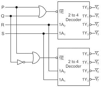
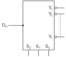
A 1 to 8 demultiplexer with data input Din, address inputs S0, S1, and S2, (with S0 as the LSB) and Y̅0 to Y̅ 7 as the eight de-multiplexed output, is to be designed using two 2 to 4 decoders (with enable input E and address input A0 and A1) as shown in the figure. Din, S0, S1, and S2 are to be connected to P, Q, R, and S but not necessarily in this order. The respective input connections to P, Q, R, and S terminals should be

- a)S2, Din, S0, and S1
- b)S1, Din,, S0, and S2
- c)Din,, S0, S1, and S2
- d)Din, S2, S0, and S1
Correct answer is option 'D'. Can you explain this answer?
| FREE This question is part of | Download PDF Attempt this Test |
Verified Answer
A 1 to 8 demultiplexer with data input Din,address inputs S0, S1, and ...
The given question is the expansion of
2 : 4 decoder to 1 : 8 decoder

We need to implement 1 : 8 DEMUX.
So, select lines of De-Mux should be mapped to address lines of the decoder.
The LSB of De-Mux should be connected to the LSB of address lines of the decoder
∴ R → S0
and S→ S1
Input to both the decoder should be same so
∴ P → Din
∴ NOT gate along with OR gate in case to select one decoder at a time so Q → S2
So,
P → Din
Q → S2
R → S0
S→ S1
Hence option (D) is correct
Most Upvoted Answer
A 1 to 8 demultiplexer with data input Din,address inputs S0, S1, and ...
The given question is the expansion of
2 : 4 decoder to 1 : 8 decoder

We need to implement 1 : 8 DEMUX.
So, select lines of De-Mux should be mapped to address lines of the decoder.
The LSB of De-Mux should be connected to the LSB of address lines of the decoder
∴ R → S0
and S→ S1
Input to both the decoder should be same so
∴ P → Din
∴ NOT gate along with OR gate in case to select one decoder at a time so Q → S2
So,
P → Din
Q → S2
R → S0
S→ S1
Hence option (D) is correct
Attention Electrical Engineering (EE) Students!
To make sure you are not studying endlessly, EduRev has designed Electrical Engineering (EE) study material, with Structured Courses, Videos, & Test Series. Plus get personalized analysis, doubt solving and improvement plans to achieve a great score in Electrical Engineering (EE).

|
Explore Courses for Electrical Engineering (EE) exam
|

|
Similar Electrical Engineering (EE) Doubts
A 1 to 8 demultiplexer with data input Din,address inputs S0, S1, and S2, (with S0as the LSB) and Y0to Y7as the eight de-multiplexed output, is to be designed using two 2 to 4 decoders (with enable input Eand address input A0and A1) as shown in the figure. Din, S0, S1, and S2are to be connected to P, Q, R, and Sbut not necessarily in this order. The respective input connections to P, Q, R, and Sterminals should bea)S2,Din,S0,and S1b)S1, Din,, S0, and S2c)Din,, S0, S1, and S2d)Din, S2, S0, and S1Correct answer is option 'D'. Can you explain this answer?
Question Description
A 1 to 8 demultiplexer with data input Din,address inputs S0, S1, and S2, (with S0as the LSB) and Y0to Y7as the eight de-multiplexed output, is to be designed using two 2 to 4 decoders (with enable input Eand address input A0and A1) as shown in the figure. Din, S0, S1, and S2are to be connected to P, Q, R, and Sbut not necessarily in this order. The respective input connections to P, Q, R, and Sterminals should bea)S2,Din,S0,and S1b)S1, Din,, S0, and S2c)Din,, S0, S1, and S2d)Din, S2, S0, and S1Correct answer is option 'D'. Can you explain this answer? for Electrical Engineering (EE) 2024 is part of Electrical Engineering (EE) preparation. The Question and answers have been prepared according to the Electrical Engineering (EE) exam syllabus. Information about A 1 to 8 demultiplexer with data input Din,address inputs S0, S1, and S2, (with S0as the LSB) and Y0to Y7as the eight de-multiplexed output, is to be designed using two 2 to 4 decoders (with enable input Eand address input A0and A1) as shown in the figure. Din, S0, S1, and S2are to be connected to P, Q, R, and Sbut not necessarily in this order. The respective input connections to P, Q, R, and Sterminals should bea)S2,Din,S0,and S1b)S1, Din,, S0, and S2c)Din,, S0, S1, and S2d)Din, S2, S0, and S1Correct answer is option 'D'. Can you explain this answer? covers all topics & solutions for Electrical Engineering (EE) 2024 Exam. Find important definitions, questions, meanings, examples, exercises and tests below for A 1 to 8 demultiplexer with data input Din,address inputs S0, S1, and S2, (with S0as the LSB) and Y0to Y7as the eight de-multiplexed output, is to be designed using two 2 to 4 decoders (with enable input Eand address input A0and A1) as shown in the figure. Din, S0, S1, and S2are to be connected to P, Q, R, and Sbut not necessarily in this order. The respective input connections to P, Q, R, and Sterminals should bea)S2,Din,S0,and S1b)S1, Din,, S0, and S2c)Din,, S0, S1, and S2d)Din, S2, S0, and S1Correct answer is option 'D'. Can you explain this answer?.
A 1 to 8 demultiplexer with data input Din,address inputs S0, S1, and S2, (with S0as the LSB) and Y0to Y7as the eight de-multiplexed output, is to be designed using two 2 to 4 decoders (with enable input Eand address input A0and A1) as shown in the figure. Din, S0, S1, and S2are to be connected to P, Q, R, and Sbut not necessarily in this order. The respective input connections to P, Q, R, and Sterminals should bea)S2,Din,S0,and S1b)S1, Din,, S0, and S2c)Din,, S0, S1, and S2d)Din, S2, S0, and S1Correct answer is option 'D'. Can you explain this answer? for Electrical Engineering (EE) 2024 is part of Electrical Engineering (EE) preparation. The Question and answers have been prepared according to the Electrical Engineering (EE) exam syllabus. Information about A 1 to 8 demultiplexer with data input Din,address inputs S0, S1, and S2, (with S0as the LSB) and Y0to Y7as the eight de-multiplexed output, is to be designed using two 2 to 4 decoders (with enable input Eand address input A0and A1) as shown in the figure. Din, S0, S1, and S2are to be connected to P, Q, R, and Sbut not necessarily in this order. The respective input connections to P, Q, R, and Sterminals should bea)S2,Din,S0,and S1b)S1, Din,, S0, and S2c)Din,, S0, S1, and S2d)Din, S2, S0, and S1Correct answer is option 'D'. Can you explain this answer? covers all topics & solutions for Electrical Engineering (EE) 2024 Exam. Find important definitions, questions, meanings, examples, exercises and tests below for A 1 to 8 demultiplexer with data input Din,address inputs S0, S1, and S2, (with S0as the LSB) and Y0to Y7as the eight de-multiplexed output, is to be designed using two 2 to 4 decoders (with enable input Eand address input A0and A1) as shown in the figure. Din, S0, S1, and S2are to be connected to P, Q, R, and Sbut not necessarily in this order. The respective input connections to P, Q, R, and Sterminals should bea)S2,Din,S0,and S1b)S1, Din,, S0, and S2c)Din,, S0, S1, and S2d)Din, S2, S0, and S1Correct answer is option 'D'. Can you explain this answer?.
Solutions for A 1 to 8 demultiplexer with data input Din,address inputs S0, S1, and S2, (with S0as the LSB) and Y0to Y7as the eight de-multiplexed output, is to be designed using two 2 to 4 decoders (with enable input Eand address input A0and A1) as shown in the figure. Din, S0, S1, and S2are to be connected to P, Q, R, and Sbut not necessarily in this order. The respective input connections to P, Q, R, and Sterminals should bea)S2,Din,S0,and S1b)S1, Din,, S0, and S2c)Din,, S0, S1, and S2d)Din, S2, S0, and S1Correct answer is option 'D'. Can you explain this answer? in English & in Hindi are available as part of our courses for Electrical Engineering (EE).
Download more important topics, notes, lectures and mock test series for Electrical Engineering (EE) Exam by signing up for free.
Here you can find the meaning of A 1 to 8 demultiplexer with data input Din,address inputs S0, S1, and S2, (with S0as the LSB) and Y0to Y7as the eight de-multiplexed output, is to be designed using two 2 to 4 decoders (with enable input Eand address input A0and A1) as shown in the figure. Din, S0, S1, and S2are to be connected to P, Q, R, and Sbut not necessarily in this order. The respective input connections to P, Q, R, and Sterminals should bea)S2,Din,S0,and S1b)S1, Din,, S0, and S2c)Din,, S0, S1, and S2d)Din, S2, S0, and S1Correct answer is option 'D'. Can you explain this answer? defined & explained in the simplest way possible. Besides giving the explanation of
A 1 to 8 demultiplexer with data input Din,address inputs S0, S1, and S2, (with S0as the LSB) and Y0to Y7as the eight de-multiplexed output, is to be designed using two 2 to 4 decoders (with enable input Eand address input A0and A1) as shown in the figure. Din, S0, S1, and S2are to be connected to P, Q, R, and Sbut not necessarily in this order. The respective input connections to P, Q, R, and Sterminals should bea)S2,Din,S0,and S1b)S1, Din,, S0, and S2c)Din,, S0, S1, and S2d)Din, S2, S0, and S1Correct answer is option 'D'. Can you explain this answer?, a detailed solution for A 1 to 8 demultiplexer with data input Din,address inputs S0, S1, and S2, (with S0as the LSB) and Y0to Y7as the eight de-multiplexed output, is to be designed using two 2 to 4 decoders (with enable input Eand address input A0and A1) as shown in the figure. Din, S0, S1, and S2are to be connected to P, Q, R, and Sbut not necessarily in this order. The respective input connections to P, Q, R, and Sterminals should bea)S2,Din,S0,and S1b)S1, Din,, S0, and S2c)Din,, S0, S1, and S2d)Din, S2, S0, and S1Correct answer is option 'D'. Can you explain this answer? has been provided alongside types of A 1 to 8 demultiplexer with data input Din,address inputs S0, S1, and S2, (with S0as the LSB) and Y0to Y7as the eight de-multiplexed output, is to be designed using two 2 to 4 decoders (with enable input Eand address input A0and A1) as shown in the figure. Din, S0, S1, and S2are to be connected to P, Q, R, and Sbut not necessarily in this order. The respective input connections to P, Q, R, and Sterminals should bea)S2,Din,S0,and S1b)S1, Din,, S0, and S2c)Din,, S0, S1, and S2d)Din, S2, S0, and S1Correct answer is option 'D'. Can you explain this answer? theory, EduRev gives you an
ample number of questions to practice A 1 to 8 demultiplexer with data input Din,address inputs S0, S1, and S2, (with S0as the LSB) and Y0to Y7as the eight de-multiplexed output, is to be designed using two 2 to 4 decoders (with enable input Eand address input A0and A1) as shown in the figure. Din, S0, S1, and S2are to be connected to P, Q, R, and Sbut not necessarily in this order. The respective input connections to P, Q, R, and Sterminals should bea)S2,Din,S0,and S1b)S1, Din,, S0, and S2c)Din,, S0, S1, and S2d)Din, S2, S0, and S1Correct answer is option 'D'. Can you explain this answer? tests, examples and also practice Electrical Engineering (EE) tests.

|
Explore Courses for Electrical Engineering (EE) exam
|

|
Suggested Free Tests
Signup for Free!
Signup to see your scores go up within 7 days! Learn & Practice with 1000+ FREE Notes, Videos & Tests.


