Current Source Inverters | Power Electronics - Electrical Engineering (EE) PDF Download
Introduction
The inverters are used to convert the power from dc to ac. The voltage source inverter (VSI) and current source inverter (CSI) are two types of inverters, the main difference between voltage source inverter and current source inverter is that the output voltage is constant in VSI and the input current is constant in CSI. The CSI is a constant current source which supplies ac to the input, and it is also called dc-link converter in which load current is constant. This article discusses the current source inverter.
Current Source Inverter
The current source inverter is also known as current fed inverter which converts the input dc into ac and its output can be three-phase or single phase. According to the definition of the current source, an ideal current source is the kind of source in which current is constant and it is independent of voltage.
Current Source Inverter Control
The voltage source is connected in series with a large value of inductance (Ld) and this named the circuit as the current source. The circuit diagram of the current source inverter fed induction motor drive is shown in the below figure.
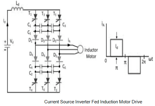
The circuit consists of six diodes (D1, D2, D3, D4, D5, D6), six capacitors (C1, C2, C3, C4, C5, C6), six thyristors (T1, T2, T3, T4, T5, T6) which are fixed with a phase difference of 60°. The inverter output is connected to the induction motor. For a given speed, torque is controlled by varying the dc-link current Id and this current can be varied by varying the Vd. The conduction of two switches in the same lag doesn’t lead to a sudden rise of current due to the presence of a large value of inductance Ld.
The configurations of current source inverter fed inductor motor drive depending upon the source are shown in the below figure.
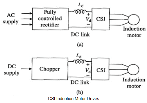
When the source is available in dc source, the chopper is used to vary the current. When the source is available in ac source then there fully controlled rectifier is used to vary the output current.
Closed Loop Slip Controlled CSI Drive With Regenerative Barking
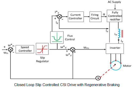
The reference speed of the motor error (∆ωm) is given to the speed controller which is normally VI controller and the output of VI controller is the slip speed that is given to the slip regulator which is required to regulate the speed. The slip speed is given to the flux control and the output of this is reference current Id* that must be controlled. The slip speed (ωms) and actual speed (ωm) are added and will get the synchronous speed, from the synchronous speed we can determine the frequency.
The frequency command is given to the CSI because the inverter is very much capable of controlling the frequency. We can control the output of CSI by changing the input current. The reference current( Id*) and actual current ( Id) is added and will get the error of the current (∆ Id). The error of the current is given to the current controller which controls the dc-link current and based on the dc-link current we can control the α, and this α will decide the voltage based on which you can determine, that how much current is going to change. This is the closed-loop slip controlled CSI drive with regenerative braking. This is the operation of a closed-loop slip controlled CSI drive with regenerative braking and its circuit diagram is shown in the below figure.
The main advantage of CSI fed drive is, it is more reliable than voltage source inverter fed drive and the disadvantage is, it has a lower speed range, slower dynamic response, the drive operates always in closed-loop and it is not suitable for multi-motor drive.
Current Source Inverter with R-Load
The circuit diagram of the current source inverter with R-load is shown in the below figure.
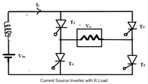
The circuit consists of four thyristor switches (T1, T2, T3, T4), IS is the input source current which is constant, and you can see that there is no any anti-parallel diode is connected. The constant current is provided by connecting voltage sources in series with large inductance. We know that the property of inductance, that it won’t allow the sudden change in current, so when we connect voltage source with large inductance then definitely the current produced across it will be constant. The fundamental dissipation factor of the current source inverter with resistive load is equal to one.
Parameters of the Current Source Inverter with R-Load
If we trigger T1 and T2 from 0 to T/2 then the output current and the output voltage is expressed as
I0 = IS > 0
V0 = I0R
If we trigger T3 and T4 from T/2 to T then the output current and the output voltage is expressed as
I0 = -IS > 0
V0 = I0R < 0
The output waveform of the current source inverter with R-load is shown in the below figure
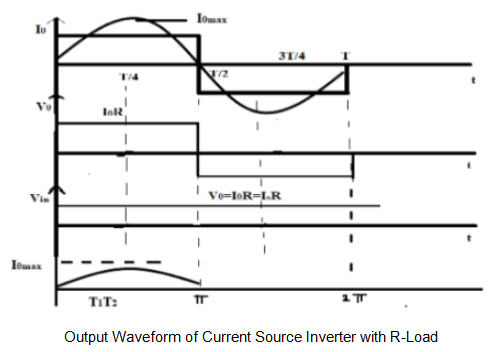
In the case of resistive load, forced commutation is required. From 0 to T/2, T1 and T2 are conducting and from T/2 to T, T3 & T4 are conducting. So, the conduction angle of each switch will be equal to ᴨ and the conduction time of each switch will be equal to T/2.
The input voltage of the resistive load is expressed as
Vin = V0 (from 0 to T/2)
Vin = -V0 (from T/2 to T)
The RMS output current and the RMS output voltage of the CSI resistive load is expressed as
I0(RMS) = IS
V0(RMS) = I0(RMS)R
The average and RMS thyristor current of the CSI with resistive load is
IT(avg) = IS/2
IT(RMS) = IS/√2
The Fourier series of output current and the output voltage of the CSI with resistive load is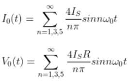
The fundamental component of the RMS output current is
I01(RMS) = 2√2/ᴨ * IS
The distortion factor of the current source inverter with R-load is
g = 2√2/ᴨ
The total harmonic distortion is expressed as
THD=48.43%
The fundamental component of average and RMS thyristor current is
IT01(avg) = I01(max)/ ᴨ
IT01(RMS)=I01(max)/ 2
The fundamental power across the load is expressed as
V01(RMS) * I01(RMS) * cosϕ1
The total power across the load is expressed as
I0(RMS)2 R = V0(RMS)2/ R
The input voltage Vin is always positive because the power is always delivered from source to load.
Current Source Inverter with Capacitive load or C-load
The circuit diagram of the current source inverter capacitive load is shown in the below figure
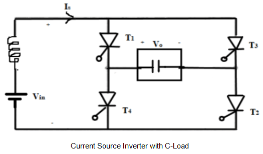
In the waveform from o to T/2, T1 and T2 are triggered and the output current is I0=IS. Similarly from T/2 to T, T3 and T4 are triggered and the output current is I0=-IS. So load current waveform is not depending upon load. The output waveform of CSI inverter with C-Load is shown in the below figure.
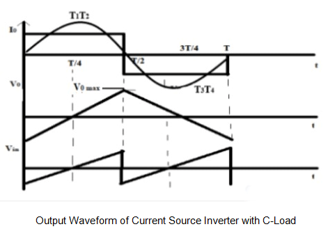
The integration of the output current waveform will give the output voltage. If the output current is ac then definitely the output voltage is ac. In the circuit diagram, the purely capacitive load is taken, so the current leads the voltage by 90°.
I0 = IC = C dV0/dt
V0(t) = 1/C ∫IC(t) dt=1/C ∫I0 dt
The input voltage of the C-load is
Vin = V0 (from 0 to T/2)
Vin = -V0 (from T/2 to T)
The output voltage is positive when T1 and T2 are conducting from 0 to π and when T3 and T4 conducting from π to 3π/2 then by default the T1 and T2 are going into reverse bias because of the positive voltage load, that means in this case natural commutation or load commutation is possible, means we don’t need to put an external circuit or external commutation circuit in order to turn off the thyristor T1 and T2. We need to find the circuit turnoff time when natural commutation is possible. The circuit turnoff time is expressed as
ω0 tc = ᴨ/2
tc = ᴨ/2 ω0
Parameters of the Current Source Inverter with C-Load
The average and RMS thyristor current is expressed as
IT(avg) = IS/2
IT(RMS) = IS/√2
The Fourier series of output current and the output voltage of the capacitive load is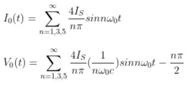
The fundamental dissipation factor of CSI with C-load is equal to zero.
The fundamental component of output power is expressed as
P01 = V01(RMS) I01(RMS) Cos ϕ1 = 0
The fundamental component of average and RMS thyristor current is
IT01(avg)= I01(max)/ ᴨ and IT01(RMS)=I01(max)/ 2
The maximum output voltage is
V0(max) = IST/4C
The RMS value of the input voltage is
Vin(RMS)=Vo(max)/ √3
These are the parameters of the current source inverter with the capacitive load.
Applications
The applications of current source inverter are
- UPS units
- LT plasma generators
- AC motor drives
- Switching devices
- Induction motors for pumps and fans
Advantages
The advantages of the current source inverter are
- Feedback diode is not required
- Commutation is simple
Disadvantages
The disadvantages of the current source inverter are
- It needs an extra converter stage
- At light load, it has stability problem and sluggish performance
|
5 videos|51 docs|46 tests
|


