Physics Exam  >  Physics Notes  >  Solid State Physics, Devices & Electronics  >  Operational Amplifier - Assignment

Operational Amplifier - Assignment | Solid State Physics, Devices & Electronics PDF Download

Q.1. (a) An op-amp has CMRR = 100dB , differential gain A= 5 and common mode voltage applied to it is 3 mV . Find the value of common mode output voltage.
(b) An op-amp has differential gain AD = 100 . Common mode voltage applied to it is 3 mV and corresponding output voltage is 0.03 μV . Find the value of CMRR in dB.

(a) CMRR(in dB) = 20log10(AD/ACM)
Operational Amplifier - Assignment | Solid State Physics, Devices & Electronics
∵ ACM = VoCM/VCM = 5 x 10⁻⁵ ⇒VoCM = 5 x 10-5 x 3 x 10-3V = 15 x 10-8V = 0.15μV
Operational Amplifier - Assignment | Solid State Physics, Devices & Electronics


Q.2. Consider the circuit shown in figure below.
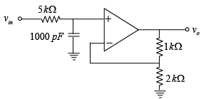
Operational Amplifier - Assignment | Solid State Physics, Devices & Electronics(a) Find the frequency above which the gain will decrease by 20 dB per decade.
(b) Find the magnitude of gain at operating frequency of 40 kHz.
(c) Find the phase angle (∅) at 40 kHz.

Operational Amplifier - Assignment | Solid State Physics, Devices & Electronics


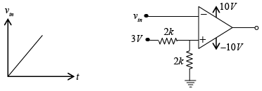
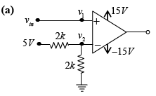
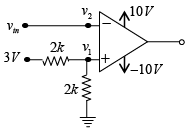
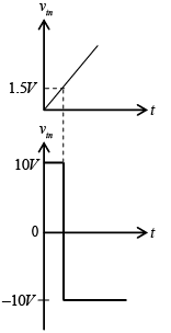
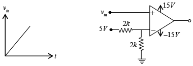
Q.3. For the circuit shown in figure draw output waveform.
(a) 
Operational Amplifier - Assignment | Solid State Physics, Devices & Electronics
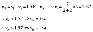
(b)
Operational Amplifier - Assignment | Solid State Physics, Devices & Electronics

Operational Amplifier - Assignment | Solid State Physics, Devices & Electronics
Operational Amplifier - Assignment | Solid State Physics, Devices & Electronicsvid = v1 - v2 = vin - 2.5V ∵ Operational Amplifier - Assignment | Solid State Physics, Devices & Electronics
∵ vin < 2.5V ⇒ vid = -ve
∵ vin > 2.5V ⇒ vid = +ve
(b) Operational Amplifier - Assignment | Solid State Physics, Devices & Electronics
Operational Amplifier - Assignment | Solid State Physics, Devices & ElectronicsOperational Amplifier - Assignment | Solid State Physics, Devices & Electronics


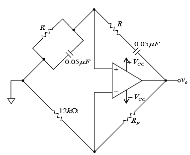
Q.4. Consider the circuit shown in figure below.
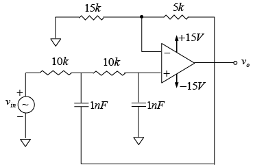
Operational Amplifier - Assignment | Solid State Physics, Devices & Electronics(a) Find the frequency above which the gain will decrease by 40 dB per decade.
(b) Find the magnitude of gain at operating frequency of 20 kHz.

Operational Amplifier - Assignment | Solid State Physics, Devices & Electronics


Q.5. An amplifier has a voltage gain of 500, input impedance 20 kΩ, output impedance 75 Ω and bandwidth is 10 Hz without any feedback. Now a negative feedback with β = 0.1 is applied. Find
(a) Its gain
(b) Input impedance
(c) Output impedance
(d) Its bandwidth

Operational Amplifier - Assignment | Solid State Physics, Devices & Electronics
(b) RiF = Ri (1 + AB) = 20k x (1 + 500 x 0.1) = 1020kΩ
(c) RoF = R0/(1+AB) = 75/(1 + 500 x 0.1) = 1.5Ω
(d) foF = f0(1+AB) = 10(1 + 500 x 0.1) = 510Hz


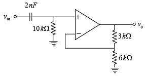
Q.6. Consider the circuit shown in figure below.
Operational Amplifier - Assignment | Solid State Physics, Devices & Electronics

(a) Find the frequency upto which the gain will increase by 20 dB per decade.
(b) Find the magnitude of gain at operating frequency 4 kHz and 6 kHz.
(c) Find the phase angle (∅) at 6 kHz.

Operational Amplifier - Assignment | Solid State Physics, Devices & Electronics
At 4kHz, Operational Amplifier - Assignment | Solid State Physics, Devices & Electronics
At 6kHz, Operational Amplifier - Assignment | Solid State Physics, Devices & Electronics
(c) Operational Amplifier - Assignment | Solid State Physics, Devices & Electronics


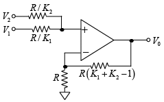
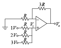
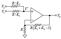
Q.7. Find the output voltage V0 of the OPAMP circuit shown in figure below
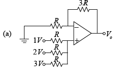
Operational Amplifier - Assignment | Solid State Physics, Devices & Electronics
(b)
Operational Amplifier - Assignment | Solid State Physics, Devices & Electronics

Operational Amplifier - Assignment | Solid State Physics, Devices & Electronics
⇒ V0 = 8V

Operational Amplifier - Assignment | Solid State Physics, Devices & Electronics

(b) Operational Amplifier - Assignment | Solid State Physics, Devices & Electronics
Operational Amplifier - Assignment | Solid State Physics, Devices & Electronics
⇒ V0 = K1V1 + K2V2
Operational Amplifier - Assignment | Solid State Physics, Devices & Electronics


Q.8. Consider the circuit shown in figure below.
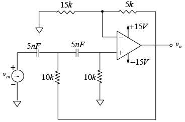
Operational Amplifier - Assignment | Solid State Physics, Devices & Electronics

(a) Find the frequency upto which the gain will increase by 40 dB per decade.
(b) Find the magnitude of gain at operating frequency of 2 kHz.

Operational Amplifier - Assignment | Solid State Physics, Devices & Electronics


Q.9. In an ideal Op-Amp circuit shown below Vi = Vm sinωt.
(a) Find the amplitude of V0.
(b) Find the peak value of current through R1.
(c) Find the peak value of current through R2 .
(c) Find the peak value of potential at P. 
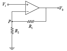
Operational Amplifier - Assignment | Solid State Physics, Devices & Electronics

Operational Amplifier - Assignment | Solid State Physics, Devices & Electronics
(b) Current through R1 is Operational Amplifier - Assignment | Solid State Physics, Devices & Electronics
Peak value of current = Vm/R2
(c) Current through R2 is Operational Amplifier - Assignment | Solid State Physics, Devices & Electronics
Peak value of current = Vm/R2
(d) Peak value of voltage at P is = Vm.


Q.10. The input to a lock-in amplifier has the form Vi(t) = Vi sin(ωt+60) where Vi, ω and 600 are the amplitude, frequency and phase of the input signal respectively. This signal is multiplied by a reference signal of the same frequency ω, amplitude Vr and phase 300.
(a) If the multiplied signal is fed to a high pass filter of cut-off frequency ω, find the final 
output signal.

(a) If the multiplied signal is fed to a low pass filter of cut-off frequency ω, find the final output signal.

(b) If the multiplied signal is fed to a High pass filter of cut-off frequency ω, find the final output signal.

V = Vrsin(ωt+30) x Visin(ωt+60) = ViVr/2[cos(60-30) -cos(2ωt+60+30)]

Operational Amplifier - Assignment | Solid State Physics, Devices & Electronics
(a) Output of Low pass filter Operational Amplifier - Assignment | Solid State Physics, Devices & Electronics
(b) Output of high pass filter Operational Amplifier - Assignment | Solid State Physics, Devices & Electronics


Q.11. For the circuit shown in figure the output is Vo = -2V1 +3V2 - V3. Find the values of resistances R1, R2 and R3.
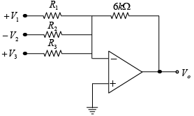
Operational Amplifier - Assignment | Solid State Physics, Devices & Electronics

Operational Amplifier - Assignment | Solid State Physics, Devices & Electronics
⇒ Vo = -2V1 + 3V2 - V3
Thus R1 = 3kΩ, R2 = 2kΩ and R3 = 6kΩ.


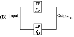
Q.12. Consider a Low Pass (LP) and a High Pass (HP) filter with cut-off frequencies fLP and fHP, respectively, connected in series or in parallel configurations as shown in the Figures A and B below. 

Operational Amplifier - Assignment | Solid State Physics, Devices & ElectronicsOperational Amplifier - Assignment | Solid State Physics, Devices & Electronics

Find the response of Filter A and B if
(a) fHP < FLP (b) fHP > f
LP

(a) fHP < FLP
A acts as a Band Pass filter, B allows the signal from passing through
(b) fHP > fLP
A stops the signal from passing through, B acts as a Band Reject filter


Q.13. For the circuit shown in figure R1 = R2 = R= 2Ω, L = 1μH and C = 1μF . If the input is vin = cos(106t), then |v0/vin| is
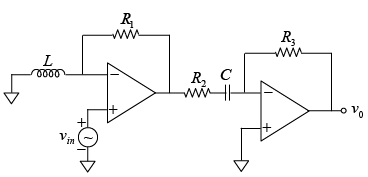
Operational Amplifier - Assignment | Solid State Physics, Devices & Electronics

Output of first Op-Amp is Operational Amplifier - Assignment | Solid State Physics, Devices & Electronics
Operational Amplifier - Assignment | Solid State Physics, Devices & Electronics
Output of second Op-Amp is Operational Amplifier - Assignment | Solid State Physics, Devices & Electronics
Operational Amplifier - Assignment | Solid State Physics, Devices & Electronics


Q.14. Consider the Op-Amp circuit shown in figure.
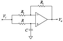
Operational Amplifier - Assignment | Solid State Physics, Devices & Electronics

If Vi = V1sin(ωt) and V= V2 sin(ωt + ∅), then find
(a) magnitude of the gain
(b) the phase angle (∅) at ω → 0 and w → ∞.

Operational Amplifier - Assignment | Solid State Physics, Devices & Electronics

Thus ∅ = -2tan-1(ωRC).
(a) Magnitude of the gain is 1.
(b) The phase angle (∅) at w → 0 is ∅ = 0 and at ω → ∞ is ∅ = -π.


Q.15. In the op-amp circuit shown in the figure, Vi is a sinusoidal input signal of frequency 10 Hz and Vo is the output signal.
(a) Find the magnitude of the gain.
(b) Find the phase of the output signal.
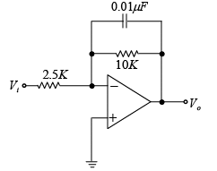
Operational Amplifier - Assignment | Solid State Physics, Devices & Electronics

Operational Amplifier - Assignment | Solid State Physics, Devices & Electronics
Operational Amplifier - Assignment | Solid State Physics, Devices & Electronics Operational Amplifier - Assignment | Solid State Physics, Devices & Electronics
(b) Phase of the output signal ∅ = π - θ = π - tan-(ωCRF)
θ = tan-1 (2 x 3.14 x 10 x 10-8 x 104) = tan-1 (6.28 x 10⁻³) ≈ 0
⇒ ∅ = π - θ ≈ π


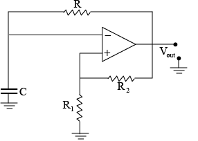
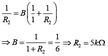
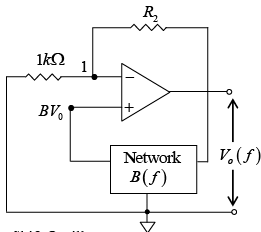
Q.16. The circuit in figure employs positive feedback and is intended to generate sinusoidal oscillation. If at a frequency Operational Amplifier - Assignment | Solid State Physics, Devices & Electronics then to sustain oscillation at this frequency find R2.
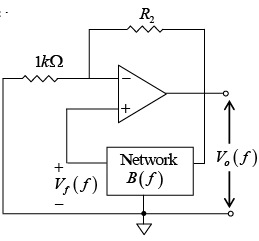
Operational Amplifier - Assignment | Solid State Physics, Devices & Electronics

Apply KCL at node 1
Operational Amplifier - Assignment | Solid State Physics, Devices & Electronics

Operational Amplifier - Assignment | Solid State Physics, Devices & Electronics


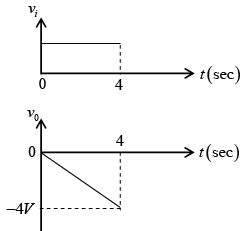
Q.17. Figure shows a practical integrator with RS = 30MΩ, RF = 20MΩ and CF = 0.1μF. If a step (dc) voltage of +3V is applied as input for 0 ≤ t ≤ 4 (t is in seconds), then draw output voltage as a function of input voltage.
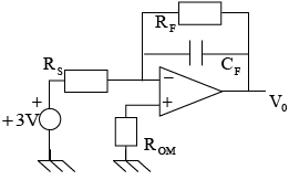
Operational Amplifier - Assignment | Solid State Physics, Devices & Electronics

Operational Amplifier - Assignment | Solid State Physics, Devices & Electronics
⇒ V0 = -t Volts
A ramp function of peak voltage -4V.
Operational Amplifier - Assignment | Solid State Physics, Devices & Electronics


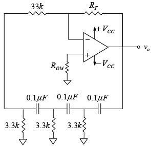
Q.18. For the circuit in shown in figure below find output frequency frequency f0 and resistance RF

Operational Amplifier - Assignment | Solid State Physics, Devices & Electronics

The circuit shown in figure is Phase Shift Oscillator.
The frequency of oscillation f0 and is given by
Operational Amplifier - Assignment | Solid State Physics, Devices & Electronics 
At this frequency, the gain Au must be at least 29. That is, Operational Amplifier - Assignment | Solid State Physics, Devices & Electronics
⇒ RF = 957kΩ


Q.19. In the Op-Amp circuit shown, assume that the diode current follows the equation I = I0exp(V/VT). For Vi = 2V, V0 = V01 and for V= 8V, Vo = V02. At room temperature of 270 C find the value of (V01-V02).
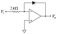
Operational Amplifier - Assignment | Solid State Physics, Devices & Electronics

Operational Amplifier - Assignment | Solid State Physics, Devices & Electronics
At room temperature of 270C, VT = 26mV
⇒ V01 - V02 = 2VT ln 2 = 2 x 26 x 0.693mV ≈ 36mV


Q.20. For the circuit in shown in figure below if output frequency frequency f0 = 965Hz find R and RF

Operational Amplifier - Assignment | Solid State Physics, Devices & Electronics

The circuit shown in figure is Wein Bridge Oscillator.
Operational Amplifier - Assignment | Solid State Physics, Devices & Electronics
At this frequency RF = 2R1 = 2 x 12 = 24kΩ


Q.21. Consider the following circuit
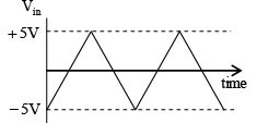
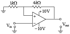
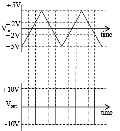
Operational Amplifier - Assignment | Solid State Physics, Devices & ElectronicsOperational Amplifier - Assignment | Solid State Physics, Devices & ElectronicsDraw output Vout corresponding to the input Vin.

Operational Amplifier - Assignment | Solid State Physics, Devices & Electronics 
Operational Amplifier - Assignment | Solid State Physics, Devices & Electronics
It’s a inverting comparator with positive feedback. Output is forced to operate in saturation region.

Operational Amplifier - Assignment | Solid State Physics, Devices & Electronics


Q.22. The OP-AMP circuit shown in figure is a bistable multivibrator. Let the OP-AMP saturation voltages be ±10V, C = 0.01 µF, R= 200kΩ, R= 2MΩ and R = 2MΩ.
Operational Amplifier - Assignment | Solid State Physics, Devices & Electronics

(a) Calculate the positive and negative threshold voltage at the inverting terminal for which the multi-vibrator will switch to other state.
(b) Calculate the frequency of the oscillation. Sketch the voltage (VOUT) waveform.

(a) Threshold voltage Operational Amplifier - Assignment | Solid State Physics, Devices & Electronics
(b) The time period T of the output waveforms is given by Operational Amplifier - Assignment | Solid State Physics, Devices & Electronics
Operational Amplifier - Assignment | Solid State Physics, Devices & Electronics

The document Operational Amplifier - Assignment | Solid State Physics, Devices & Electronics is a part of the Physics Course Solid State Physics, Devices & Electronics.
All you need of Physics at this link: Physics
91 videos|21 docs|25 tests

FAQs on Operational Amplifier - Assignment - Solid State Physics, Devices & Electronics

1. What is an operational amplifier and how does it work?
Ans. An operational amplifier (op-amp) is an electronic device that amplifies the difference between two input voltages. It is typically used in various applications, such as signal conditioning, amplification, and filtering. The op-amp has a high gain, high input impedance, and low output impedance, which allows it to amplify signals accurately. It works by comparing the voltages at its two input terminals and producing an output voltage that is proportional to the difference between the inputs.
2. What are the key characteristics of an operational amplifier?
Ans. The key characteristics of an operational amplifier include: - High gain: An op-amp has a very high voltage gain, typically in the range of tens of thousands to hundreds of thousands. - High input impedance: The input impedance of an op-amp is very high, typically in the range of megaohms, which ensures that the input signals are not affected by the op-amp's own input impedance. - Low output impedance: The output impedance of an op-amp is very low, typically in the range of ohms, which allows it to drive loads without significant loss of signal. - Differential inputs: An op-amp has two input terminals, one for the positive input and one for the negative input. The output is proportional to the difference between these two inputs. - High common-mode rejection ratio (CMRR): The op-amp has a high CMRR, which means that it can reject any common-mode signal (i.e., a signal that is present on both inputs) and amplify only the difference between the inputs.
3. What are some common applications of operational amplifiers?
Ans. Operational amplifiers find a wide range of applications in various electronic circuits. Some common applications include: - Inverting and non-inverting amplifiers: Op-amps are often used to amplify signals in both inverting and non-inverting configurations. In the inverting configuration, the input signal is applied to the negative input terminal, while in the non-inverting configuration, the input signal is applied to the positive input terminal. - Summing amplifiers: Op-amps can be used to add multiple input signals together, creating a summing amplifier. This is commonly used in audio mixers and signal processing circuits. - Integrators and differentiators: By using external resistors and capacitors, op-amps can be used as integrators (output voltage proportional to the integral of the input voltage) and differentiators (output voltage proportional to the derivative of the input voltage). - Active filters: Op-amps can be used to build active filters that provide high-pass, low-pass, band-pass, and band-reject filtering functions. - Voltage comparators: Op-amps can be used as voltage comparators to compare two input voltages and produce a digital output based on the comparison result.
4. What is the ideal behavior of an operational amplifier?
Ans. The ideal behavior of an operational amplifier is characterized by the following: - Infinite voltage gain: The ideal op-amp has an infinite voltage gain, which means that it can amplify even the smallest input signals to any desired level. - Infinite input impedance: The ideal op-amp has an infinite input impedance, meaning that it draws zero current from the input sources. This ensures that the input signals are not affected by the op-amp's own input impedance. - Zero output impedance: The ideal op-amp has zero output impedance, allowing it to drive any load without any loss of signal. - Infinite bandwidth: The ideal op-amp has an infinite bandwidth, meaning that it can amplify signals of any frequency without distortion. - Infinite common-mode rejection ratio (CMRR): The ideal op-amp has an infinite CMRR, which means that it can completely reject any common-mode signal and amplify only the difference between the inputs.
5. What are some limitations of operational amplifiers in real-world applications?
Ans. Despite their many advantages, operational amplifiers have some limitations in real-world applications. Some of these limitations include: - Finite gain: In real op-amps, the gain is not infinite, and it can vary with frequency and temperature. This can introduce errors and affect the accuracy of the amplified signals. - Input bias current: Op-amps have a small input bias current flowing into the input terminals. This current can cause an offset voltage at the output and affect the accuracy of the amplified signal. - Input offset voltage: Op-amps have an inherent input offset voltage, which is the voltage difference between the two input terminals when the output is zero. This offset voltage can also introduce errors in the amplified signal. - Limited output voltage range: The output of an op-amp cannot exceed the power supply voltages, which limits the maximum output voltage range. - Slew rate limitation: Op-amps have a limited slew rate, which is the maximum rate of change of the output voltage. This can cause distortion in fast-changing input signals. - Frequency response limitations: Op-amps have a limited bandwidth, beyond which the gain starts to decrease. This limits the frequency range over which accurate amplification is possible.
91 videos|21 docs|25 tests
Download as PDF
Explore Courses for Physics exam
Signup for Free!
Signup to see your scores go up within 7 days! Learn & Practice with 1000+ FREE Notes, Videos & Tests.
10M+ students study on EduRev
Related Searches

Previous Year Questions with Solutions

,

Devices & Electronics

,

shortcuts and tricks

,

Sample Paper

,

Free

,

past year papers

,

MCQs

,

Operational Amplifier - Assignment | Solid State Physics

,

Summary

,

Exam

,

pdf

,

study material

,

ppt

,

Extra Questions

,

Operational Amplifier - Assignment | Solid State Physics

,

Important questions

,

mock tests for examination

,

Objective type Questions

,

Devices & Electronics

,

Semester Notes

,

video lectures

,

practice quizzes

,

Viva Questions

,

Devices & Electronics

,

Operational Amplifier - Assignment | Solid State Physics

;