Power Semiconductor Devices - 1 | Power Electronics - Electrical Engineering (EE) PDF Download
| Table of contents |
|
| Brief History of Power Electronics |
|
| Applications of Power Electronics: |
|
| Power Semiconductor Devices |
|
| Power Diodes |
|
| Power Transistors |
|
| Bipolar Junction Transistors |
|

Power engineering deals with the static and rotating power equipment for the generation, transmission and distribution of electric power. Electronics deals with the study of solid state semiconductor power devices and circuits for Power conversion to meet the desired control objectives (to control the output voltage and output power).
Power electronics may be defined as the subject of applications of solid state power semiconductor devices (Thyristors) for the control and conversion of electric power.
Power electronics deals with the study and design of Thyristorised power controllers for variety of application like Heat control, Light/Illumination control, Motor control - AC/DC motor drives used in industries, High voltage power supplies, Vehicle propulsion systems, High voltage direct current (HVDC) transmission.

Brief History of Power Electronics
The first Power Electronic Device developed was the Mercury Arc Rectifier during the year 1900. Then the other Power devices like metal tank rectifier, grid controlled vacuum tube rectifier, ignitron, phanotron, thyratron and magnetic amplifier, were developed & used gradually for power control applications until 1950.
The first SCR (silicon controlled rectifier) or Thyristor was invented and developed by Bell Lab's in 1956 which was the first PNPN triggering transistor.
The second electronic revolution began in the year 1958 with the development of the commercial grade Thyristor by the General Electric Company (GE). Thus the new era of power electronics was born. After that many different types of power semiconductor devices & power conversion techniques have been introduced.The power electronics
revolution is giving us the ability to convert, shape and control large amounts of power.
Applications of Power Electronics:
It is literally impossible to list all the applications of power electronics today; it has penetrated almost all the fields where electrical energy is in the picture. This trend is an ever increasing one especially with present trends of new devices and integrated design of power semiconductor devices and controllers. The ease of manufacturing has also led to availability of these devices in a vast range of ratings and gradually has appeared in high voltage and extra high voltage systems also. The day is not far when all of the electrical energy in the world will pass through power electronic systems.
Below is an attempt to briefly present the diaspora of power electronics.
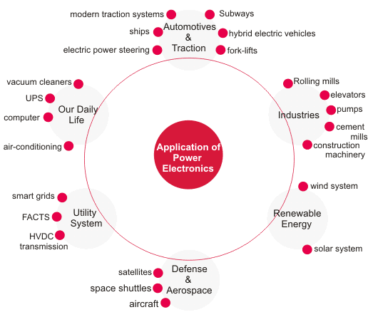 1. Commercial Applications
Heating Systems Ventilating, Air Conditioners, Central Refrigeration, Lighting, Computers and Office equipments, Uninterruptible Power Supplies (UPS), Elevators, and Emergency Lamps.
2. Domestic Applications
Cooking Equipments, Lighting, Heating, Air Conditioners, Refrigerators & Freezers, Personal Computers, Entertainment Equipments, UPS.
3. Industrial Applications
Pumps, compressors, blowers and fans. Machine tools, arc furnaces, induction furnaces, lighting control circuits, industrial lasers, induction heating, welding equipments.
4. Aerospace Applications
Space shuttle power supply systems, satellite power systems, aircraft power systems.
5. Telecommunications
Battery chargers, power supplies (DC and UPS), mobile cell phone battery chargers.
6. Transportation
Traction control of electric vehicles, battery chargers for electric vehicles, electric locomotives, street cars, trolley buses, automobile electronics including engine controls.
7. Utility Systems
High voltage DC transmission (HVDC), static VAR compensation (SVC), Alternative energy sources (wind, photovoltaic), fuel cells, energy storage systems, induced draft fans and boiler feed water pumps.
Power Semiconductor Devices
The first thyristor or the SCR was developed in 1957. The conventional Thyristors
(SCR's) were exclusively used for power control in industrial applications until 1970. After 1970, various types of power semiconductor devices were developed and became commercially available.
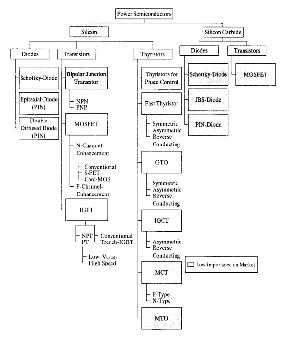 The power semiconductor devices can be divided broadly into five types:
- Power Diodes.
- Thyristors.
- Power BJT's.
- Power MOSFET's.
- Insulated Gate Bipolar Transistors (IGBT's).
- Static Induction Transistors (SIT's).
The Thyristors can be subdivided into different types:
- Forced-commutated Thyristors (Inverter grade Thyristors)
- Line-commutated Thyristors (converter-grade Thyristors)
- Gate-turn off Thyristors (GTO).
- Reverse conducting Thyristors (RCT's).
- Static Induction Thyristors (SITH).
- Gate assisted turn-off Thyristors (GATT).
- Light activated silicon controlled rectifier (LASCR) or Photo SCR's.
- MOS-Controlled Thyristors (MCT's).
Power Diodes
Power diodes are made of silicon p-n junction with two terminals, anode and cathode. P-N junction is formed by alloying, diffusion and epitaxial growth. Modern techniques in diffusion and epitaxial processes permit desired device characteristics. Fig 1 (a) and (b) shows the circuit symbol and the photograph of a typical power diode respectively.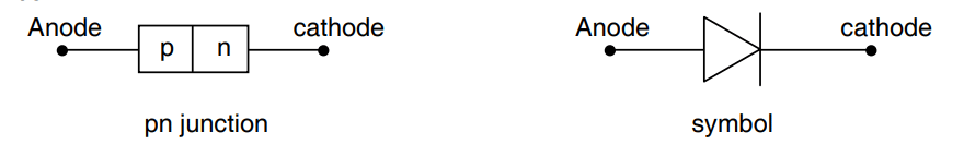 PN Junction Diode
A power diode is a two terminal p-n junction device similar to an ordinary signal diode except for its current carrying capacity. It has a low resistance to current flow in one direction (anode to cathode) and high resistance to current flow in the opposite direction (cathode to anode). The figure below shows sectional view of a pn junction and its symbol. When the anode potential is positive with respect to the cathode, the diode is said to be forward baised and this is its low resistance state. There is a small voltage drop across the diode. when the cathode potential is positive with respect to the anode, the diode is reverse biased. A small reverse current flows and this increases with the applied reverse voltage till a point when the avalanche or zener voltage is reached. The v i characteristics of the diode are expressed by the shockley equation as follows:
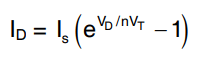
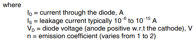
The emission coefficient n depends on the material and the physical construction of the diode. For germanium diodes n is considered 1 and for silicon it is 2. But for most practical silicon diodes it is between 1.1 to 1.8 and
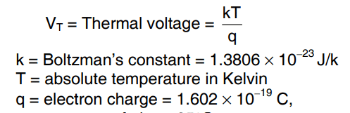
At room temperature of about 25°C, VT = 25.7 mV The diode V - I characteristics are shown in the figure.
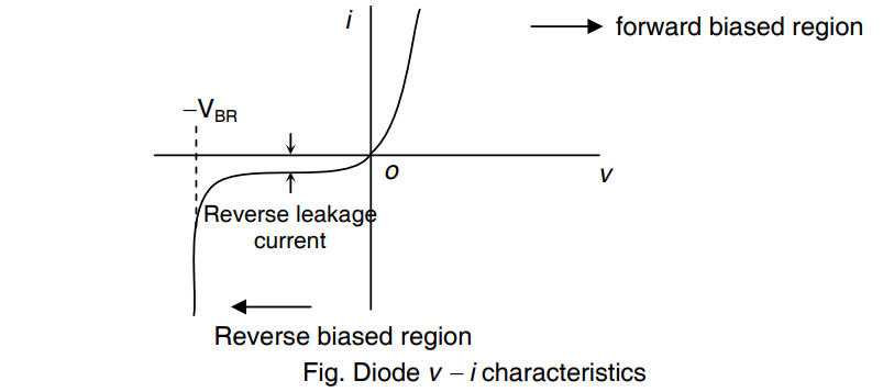
Breakdown Region : The reverse voltage is high. The breakdown voltage VBR is a voltage, where a small change in reverse voltage beyond VBR, the reverse current rises rapidly. The operation will not be destructive if power dissipation is within a safe level.
Reverse Recovery Characteristics : The current in the forward biased region is due to the net effect of majority and minority carriers. When the forward current is reduced to zero, the diode continues to conduct due to minority carriers that remain stored in the pn junction and the bulk semiconductor material. The minority carriers need some time to recombine with opposite charges to be neutralized. This time is called the reverse recovery time of the diode.
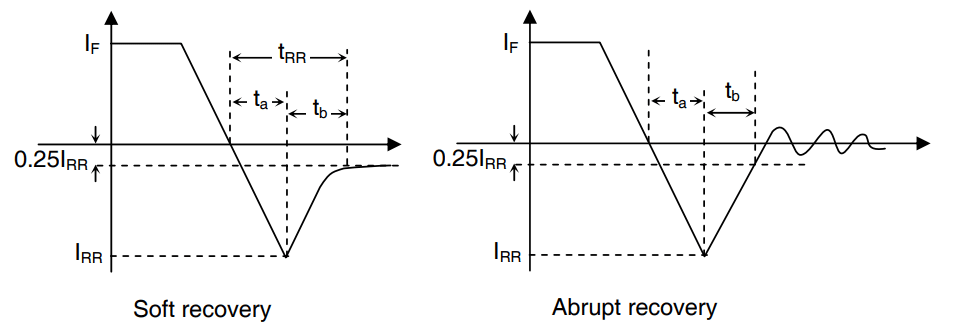 Reverse Recovery Characteristics
The diodes have the following advantages:
- High mechanical and thermal reliability
- High peak inverse voltage
- Low reverse current
- Low forward voltage drop
- High efficiency
- Compactness.
Power Transistors
Power transistors are devices that have controlled turn-on and turn-off characteristics. These devices are used a switching devices and are operated in the saturation region resulting in low on-state voltage drop. They are turned on when a current signal is given to base or control terminal. The transistor remains on so long as the control signal is present. The switching speed of modern transistors is much higher than that of thyristors and are used extensively in dc-dc and dc-ac converters. However their voltage and current ratings are lower than those of thyristors and are therefore used in low to medium power applications.
Power transistors are classified as follows
- Bipolar junction transistors(BJTs)
- Metal-oxide semiconductor filed-effect transistors(MOSFETs)
- Static Induction transistors(SITs)
- Insulated-gate bipolar transistors(IGBTs)
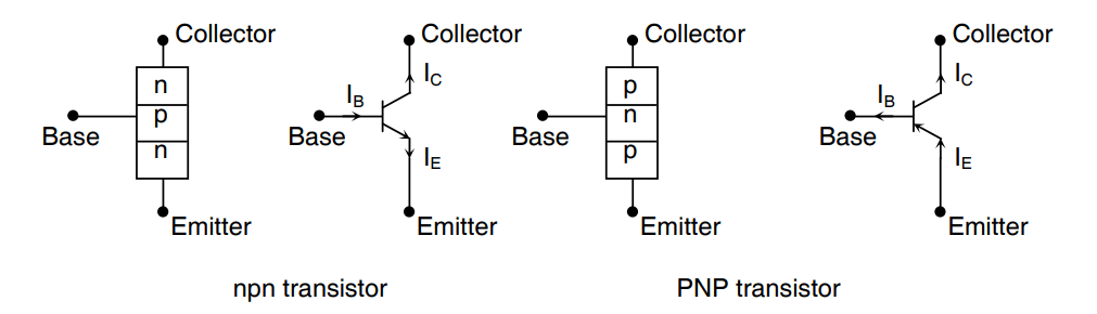
Bipolar Junction Transistors
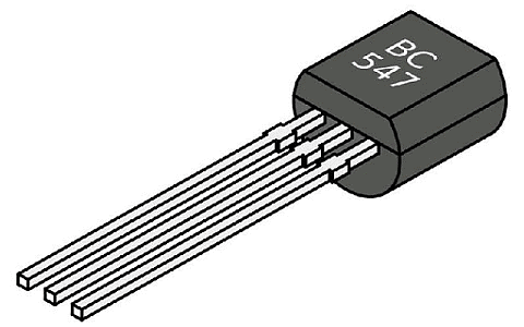 BJT IC
The need for a large blocking voltage in the off state and a high current carrying capability in the on state means that a power BJT must have substantially different structure than its small signal equivalent. The modified structure leads to significant differences in the I-V characteristics and switching behavior between power transistors and its logic level counterpart.
Structure:
If we recall the structure of conventional transistor we see a thin p-layer is sandwiched between two n-layers or vice versa to form a three terminal device with the terminals named as Emitter, Base and Collector.
The difference in the two structures is obvious.
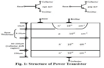
- A power transistor is a vertically oriented four layer structure of alternating p-type and n-type. The vertical structure is preferred because it maximizes the cross sectional area and through which the current in the device is flowing. This also minimizes on-state resistance and thus power dissipation in the transistor.
- The doping of emitter layer and collector layer is quite large typically 1019 cm-3. A special layer called the collector drift region (n-) has a light doping level of 1014.
- The thickness of the drift region determines the breakdown voltage of the transistor. The base thickness is made as small as possible in order to have good amplification capabilities, however if the base thickness is small the breakdown voltage capability of the transistor is compromised.
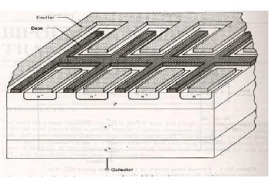
- Practical power transistors have their emitters and bases interleaved as narrow fingers as shown. The purpose of this arrangement is to reduce the effects of current crowding. This multiple emitter layout also reduces parasitic ohmic resistance in the base current path which reduces power dissipation in the transistor.
Steady State Characteristics:
Figure (a) shows the circuit to obtain the steady state characteristics. Fig (b) shows the input characteristics of the transistor which is a plot of IB versus VBE . Fig (c) shows the output characteristics of the transistor which is a plot IC versus VCE . The
characteristics shown are that for a signal level transistor.
The power transistor has steady state characteristics almost similar to signal level transistors except that the V-I characteristics has a region of quasi saturation as shown by figure 4.
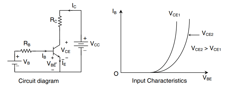 Fig (a) Circuit Diagram and (b) Input Characteristics
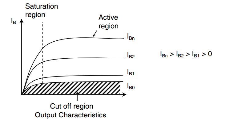 Fig (c) Output Characteristics
There are four regions clearly shown: Cutoff region, Active region, quasi saturation and hard saturation. The cutoff region is the area where base current is almost zero. Hence no collector current flows and transistor is off. In the quasi saturation and hard saturation, the base drive is applied and transistor is said to be on. Hence collector current flows depending upon the load. The power BJT is never operated in the active region (i.e. as an amplifier) it is always operated between cutoff and saturation. The BVSUS is the maximum collector to emitter voltage that can be sustained when BJT is carrying substantial collector current. The BVCEO is the maximum collector to emitter breakdown voltage that can be sustained when base current is zero and BVCBO is the collector base breakdown voltage when the emitter is open circuited
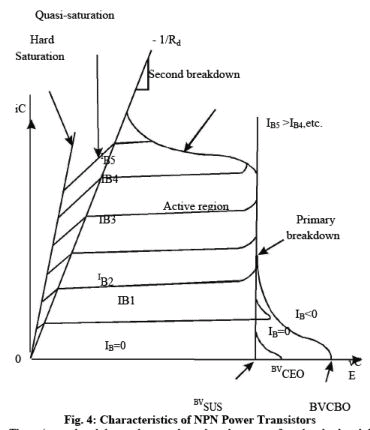
The primary breakdown shown takes place because of avalanche breakdown of collector base junction. Large power dissipation normally leads to primary breakdown.
The second breakdown shown is due to localized thermal runaway. This is explained in detail later.
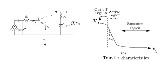
Transfer Characteristics
The transfer characteristics of a transistor refers to the graph plotting output voltage on the y-axis and the input voltage on the x- axis.
The electrical circuit and the transfer characteristics of transistor are shown above.
|
5 videos|73 docs|46 tests
|
FAQs on Power Semiconductor Devices - 1 - Power Electronics - Electrical Engineering (EE)
| 1. What are the common applications of power electronics? |  |
| 2. What are power semiconductor devices and why are they important in power electronics? | |
| 3. What is the difference between power diodes and power transistors? | |
| 4. How do bipolar junction transistors differ from other power semiconductor devices? | |
| 5. What are some factors to consider when selecting power semiconductor devices for a specific application? | |


Important questions
,Previous Year Questions with Solutions
,video lectures
,Exam
,Viva Questions
,MCQs
,Power Semiconductor Devices - 1 | Power Electronics - Electrical Engineering (EE)
,Objective type Questions
,Semester Notes
,Summary
,past year papers
,study material
,Free
,mock tests for examination
,ppt
,Power Semiconductor Devices - 1 | Power Electronics - Electrical Engineering (EE)
,Sample Paper
,practice quizzes
,Power Semiconductor Devices - 1 | Power Electronics - Electrical Engineering (EE)
,Extra Questions
,shortcuts and tricks
;


Power Semiconductor Devices - 1 Free PDF Download
Importance of Power Semiconductor Devices - 1
Power Semiconductor Devices - 1 Notes
Power Semiconductor Devices - 1 Electrical Engineering (EE) Questions
Study Power Semiconductor Devices - 1 on the App
|
© EduRev
|
Education Revolution
|


|


within 7 days!