Chapter - 5 Digital Circuits | Additional Study Material for Mechanical Engineering PDF Download
1. Number Systems & Code Conversions
Characteristics of any number system are:
- Base or radix is equal to the number of possible symbols in the system
- The largest value of digit is one (1) less than the radix
Decimal to Binary Conversion:
- Integer number: Divide the given decimal integer number repeatedly by 2 and collect the remainders. This must continue until the integer quotient becomes zero.
- Fractional Number: Multiply by 2 to give an integer and a fraction. The new fraction is multiplied by 2 to give a new integer and a new fraction. This process is continued until the fraction becomes 0 or until the numbers of digits have sufficient accuracy.
Note: To convert a decimal fraction to a number expressed in base r, a similar procedure is used. Multiplication is by r instead of 2 and the coefficients found from the integers any range in value from 0 to (r-1).
The conversion of decimal number with both integer and fraction parts separately and then combining the answers together.
- Don't care values or unused states in BCD code are 1010H1011,1100,1101,1110,1111.
- Don't care values or unused state in excess - 3 codes are 0000, 0001, 0010, 1101, 1110, 1111.
- The binary equivalent of a given decimal number is not equivalent to its BCD value. Bg. Binary equivalent o f 2Sio is equal to I I O O I 2 while BCD equivalent is 00100101.
- In signed binary numbers, MSB is always sign bit and the remaining bits are used for magnitude.

- For positive and negative binary number, the sign is respectively '0' and '1'.
- Negative numbers can be represented in one of three possible ways.
(i) Signed - magnitude representation.
(ii) Signed - 1's complement representation.
(iii) Signed - 2's complement representation.
Example: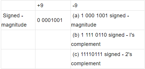
- Subtraction using 2's complement: Represent the negative numbers in signed 2's complement form, add the two numbers, including their sign bit and discard any carry out of the most significant bit.
- Since negative numbers are represented in 2's complement form, negative results also obtained in signed 2's complement form.
- The range of binary integer number of n-bits using signed l's complement form is given by +(2n-1 - 1) to -(2n-1 - 1),which includes both types of zero's i.e., +0 and -0.
- The range of integer binary numbers of n-bits length by using signed 2's complement representation is given by + (2n-1 - 1) to - 2n - 1 which includes only one type of zero i.e. + 0.
- In weighted codes, each position of the number has specific weight. The decimal value of a weighted code number is the algebraic sum of the weights of those positions in which l's appears.
- Most frequently used weighted codes are 8421, 2421 code, 5211 code and 84 2'1' code.
2. Boolean Algebra & Karnaugh Maps
- Boolean properties:
(i) Properties of AND function
1. X.0 = 0
2. 0.X = 0
3. X.1 - X
4. 1.X = X
(ii) Properties of OK function
5. X + 0 = X
6. 0 + X = X
7. X + 1 = 1
8. 1 + X = 1
(iii) Combining a variable with itself or its complement
9. X .X' = 0
10. X . X = X
11. X + X = X
12. X + X' = 1
13. (X')' = X
(iv) Commutative laws:
14. x. y = y. x
15. x + y = y + x
(v) Distributive laws:
16. x (y + z ) = x.y + x.z
17. x + y. z = ( x+y) (x + z)
(vi) Associative laws:
18. x(y.z) = (x. y) z
19. x + (y + z) = (x + y) + z
(vii) Absorption laws:
20. x + xy= x
21. x(x + y) = x
22. x + x'y = x+ y
23. x(x' + y) = xy
(viii) Demorgan's laws:
24. (x + y) f = x‘ .y'
25. (x.y)' = x' + y' - Duality principle: It states that every algebraic expression deducible from theorems of Boolean algebra remains valid if the operators and identify elements are interchanged.
- To get dual of an algebraic function, we simply exchange AND with OR and exchange 1 with 0.
- The dual of the exclusive - OR is equal to its complement.
- To find the complement of a function is take the dual of the function and complement each literal.
- Maxterm is the compliment of its corresponding minterm and vice versa.
- Sum of all the minterms of a given Boolean function is equal to 1.
- Product of all the maxterms of a given Boolean function is equal to 0.
Boolean Algebraic Theorems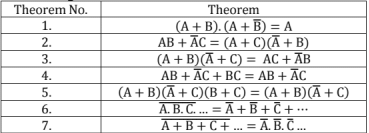
Karnaugh Maps (K - maps)
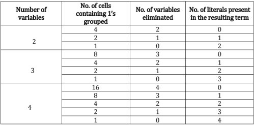
- A map is a diagram made up of squares. Each square represents either a minterm or a maxterms.
- The number of squares in the karnaugh map is given by 2n where n = number of variable.
- Gray code sequence is used in K - map so that any two adjacent cells will differ by only one bit.
3. Logic Gates
- OR, AND, NOT are basic gates
- NAND and NOR gates are called Universal gates because, by using only NAND gates or by using only NOR gates we can realize any gate or any circuit.
- EXOR, EXNOR are arithmetic gates.
- There are two types of logic systems
(i) Positive level logic system (PLLS) : Out of the given two voltage levels, the more positive value is assumed as logic T and the other as logic 'O'.
(ii) Negative level logic system (NLLS):out of the given two voltage levels, the more negative value is assumed as logic T and the other as logic 'O'. - NOT gate:-

- AND gate:

- OR gate:

- NAND gate:

- NOR gate:

- The circuit which is working as AND gate with positive level logic system, will work as OR gate with negative level logic system and vice-versa.
- The circuit which is behaving as NAND gate with positive level logic system will behave as NOR gate with negative level logic system and vice - versa.
- Exclusive OR gate (X - OR): “The output o f an X - OR gate is high for odd number of high inputs".

- Exclusive NOR gate (X-NOR): The output is high for odd number of low inputs". (OR) “The output is high for even number of high inputs".

- Realization of Basic gates using NAND and NOR gates:
(i)
(ii) AND gate
(iii) OR gate:
- Realization of NAND gate using NOR gates:

- Realization of NOR gate using NAND gates:

- Realization of X - OR gate using NAND and NOR gates:
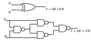

The minimum number of NAND gates required to realize X - OR gate is four.
The minimum number of NOR gates required to realize X - OR gate is five.
⇒ Equivalence Properties: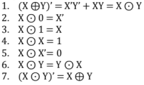
Alternate Logic Gate Symbols
(iv) A bubbled NAND gate is equivalent to OR gate
(v) A bubbled NOR gate is equivalent to AND gate
(vi) A bubbled AND gate is equivalent to NOR gate
(vii) A bubbled OR gate is equivalent to NAND gate
4. Logic Gate Families
- Fan- Out: "The number of standard loads that the output of the gate can drive without disturbing its normal operation".
- Fan-In: "The maximum number of inputs that can be applied to the logic gate".
- Noise Margin: "It is the limit of a noise voltage which may be present without impairing the proper operation of the circuit” NMH = VOH - VIH and NML = VIL - VOL.
- Figure of Merit: The product of propagation delay time and power dissipation.
- Saturation Logic: A form of logic gates in which one output state is the saturation voltage level of the transistor. Example: RTL, DTL, TTL.
- Unsaturated Logic or Current Mode Logic: A form of logic with transistors operated outside the saturation region. Example: CML or ECL.
- Voltage Parameters of the Digital IC:
VIH= This is the minimum input voltage which is recognized by the gate as logic 1.
VIL: This is the maximum input voltage which is recognized by the gate as logic 0.
VOH: This is the minimum voltage available at the output corresponding to the logic 1.
VOL: This is the maximum voltage available at the output corresponding to logic 0. - Passive Pull- up: In a bipolar logic circuit, a resistance Rc used in the collector circuit of the output transistor is known as passive pull-up.
- Active Pull-up: In a bipolar logic circuit, a BJT and diode circuit used in the collector circuit of the output transistor instead of Rc is known as active pull-up. This facility is available is TTL family.
- The advantages of active pull- up over passive- pull up are increased speed of operation and reduced power dissipation.
- In TTL logic gate family, three different types of output type configurations are available: they are open collector output type, Totem-pole output type and tri-state output type.
- The advantages of open-collector output are wired-logic can he performed and loads other than the normal gates can be used.
- The tri- state logic devices are used in bus oriented systems.
- If any input of TTL circuit is left floating, it will function as if it is connected to logic 1 level.
- If any unused input terminal of a MOS gate is left unconnected, a large voltage may get induced at the unconnected input which may damage the gate.
- Comparison of Different Logic Gate families

- Gates with open collector output can be used for wired - AND operation

- Open emitter output is available in ECL. Wired - OR operation is possible with ECL circuits.

5. Combinational Digital Circuits
Digital circuits can be classified into two types:
- Combinational digital circuits and
- Sequential digital circuits.
Combinational Digital Circuits: In these circuits "the outputs at any instant of time depends on the inputs present at that instant only."
For the design of Combinational digital circuits, basic gates (AND, OK, NOT) or universal gates (NAND, NOR) are used. Examples for combinational digital circuits are adder, decoder etc.
Sequential Digital Circuits: The outputs at any instant of time not only depend on the present inputs but also on the previous inputs or outputs. For the design of these circuits in addition to gates we need one more element called flip-flop. Examples for sequential digital circuits are Registers, Shift register, Counters etc.
Half Adder: A combinational circuit that performs the addition of two bits is called a half adder.
Sum = X ⊕ Y = XY’ + X'Y Carry = XY
Half Subtractor: It is a Combinational circuit that subtracts two bits and produces their difference.
Diff. = X ⊕ Y = XY' + X'Y Borrow = X'Y
Half adder can be converted into half subtractor with an additional inverter.
Full Adder: It performs sum of three bits (two significant bits and a previous carry) and generates sum and carry.
Sum=X⊕Y⊕Z Carry = XY + YZ + ZX
Full adder can be implemented by using two half adders and an OR gate.
Full subtractor: It subtracts one bit from the other by taking pervious borrow into account and generates difference and borrow.
Diff =X⊕ Y ⊕Z Borrow = X'T + YZ + ZX'
- Full subtractor can be implemented by using two half- subtractors and an OR gate.

Multiplexers (MUX)
- It selects binary information from one of many input lines and directs it to a single output line
- The selection of a particular input line is controlled by a set of selection lines
- There are 2n input lines where 'n' is the select lines i/p then n = log2M
2 :1 MUX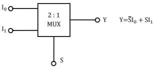
4:1 MUX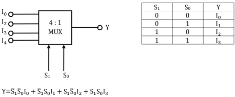
- Decoder: Decoder is a combinational circuit that converts binary information from n? input lines to a maximum of 2n unique output lines.
Truth table of active high output type of decoder.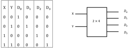
- Encoder:
• Encoder is a combinational circuit which has many inputs and many outputs
• It is used to convert other codes to binary such as octal to binary, hexadecimal to binary etc. - Clocked S-R Flip-flop: It is called set reset flip-flop.

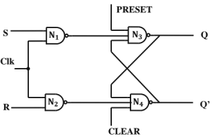
- S and R inputs are called synchronous inputs. Preset (pr) and Clear (Cr) inputs are called direct inputs or asynchronous inputs.
- The output of the flip-flop changes only during the clock pulse. In between clock pulses the output of the flip flop does not change.
- During normal operation of the flip flop, preset and clear inputs must be always high.
- The disadvantage of S-R flip-flop is S=1, R=1 output cannot be determined. This can be eliminated in J-K flip-flop.
- S-R flip flop can be converted to J-K flip-flop by using the two equation S=JQ' and R= KQ.
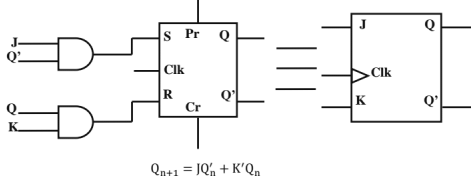
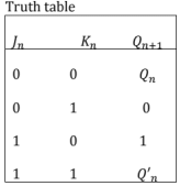
- Race around problem is present in the J-K flip flop, when both J=K-1.
- Toggling the output more than one time during the clock pulse is called Race around Problem.
- The race around problem in J-K flip-flop can be eliminated by using edge triggered flip-flop or master slave J-K flip flop or by the dock signal whose pulse width is less than or equal to the propagation delay of flip-flop.
- Master-slave flip-flop is a cascading of two J-K flip-flops Positive or direct clock pulses are applied to master and these are inverted and applied to the slave flip-flop.
D-Flip-Flop: It is also called a Delay flip-flop. By connecting an inverter in between J and K input terminals. D flip-flop is obtained.
Truth table

T Flip-flop: J K flip-flop can be converted into T- Flip-flop by connecting J and K input terminals to a common point. If T = l , then Qn+1 = Qn'. This unit changes state of the output with each clock pulse and hence it acts as a toggle switch.
Truth table

- Ring Counter: Shift register can be used as ring counter when Qo output terminal is connected to serial input terminal.
- An n-bit ring counter can have "n" different output states. It can count n-clock pulses.
- Twisted Ring counter: It is also called Johnson's Ring counter. It is formed when Qo Output terminal is connected to the serial input terminal of the shift register.
- An n-bit twisted ring counter can have maximum of 2n different output states.
Counters:-
- The counter is driven by a clock signal and can be used to count the number of clock cycles counter is nothing but a frequency divider circuit.
- Two types of counters are there:
(i) Synchronous
(ii) Asynchronous - Synchronous counters are also called parallel counters. In this type clock pulses are applied simultaneously to all the flip - flops
- Asynchronous counters are also called ripple or serial counter. In this type of counters the output of one flip - flop is connected to the clock input of next flip - flop and soon.
 |
Download the notes
Chapter - 5 Digital Circuits
|
Download as PDF |
6. AD /DA Convertor
- There are two types of DACs available
(i) Binary weighted resistor type of DAC and
(ii) R - 2 R ladder type of DAC - The advantage of R - 2R ladder type of DAC over Binary weighted type of DAC
(i) Better linearity and
(ii) It requires only two different types of resistors with values R and 2R. - The percentage resolution of n - bit DAC is given by

- The resolution of an n -bit DAC with a range of output from 0 to V volts is given by
 Volts
Volts - Different types of AD C's are available:
(i) Simultaneous ADC or parallel comparator of Flash type of ADC
(ii) Counter type ADC or pulse width type of ADC
(iii) Integrator type of ADC or single slope of ADC
(iv) Dual slope integrator ADC
(v) Successive approximation type ADC etc. - Flash type of ADC is the faster type of ADC, An n - bit Flash type ADC requires 2n - 1 comparators.
- Dual slope ADC is more accurate.
7. Semiconductor Memory
The capacity of a memory 1C is represented by 2n x m, where '2n’ represents number of memory locations available and 'm' represents number of bits stored in each memory location.
Example:- 210 x 8 = 1024 x 8
To increase the bit capacity or length of each memory location, the memory ICs are connected in parallel and the corresponding memory location of each 1C must be selected simultaneously. Eg. 1024 x 8 memory capacity can be obtained by using 4 ICs of memory capacity 1024x2.
Types of Memories: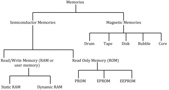
- Volatile Memory: The stores information is dependent on power supply i.e., the stored information will remain as long as power is applied. Eg. RAM
- Non- Volatile Memory: The stored information is independent of power supply i.e., the stored information will present even if the power fails. Eg: ROM, PROM, EPROM, EEPROM etc.
- Static RAM (SRAM): The binary information is stored in terms of voltage. SRAMs stores ones and zeros using conventional Flip-flops.
- Dynamic RAM (DRAM): The binary information is stored in terms of charge on the capacitor. The memory cells of DRAMs are basically charge storage capacitors with driver transistors. Because of the leakage property of the capacitor, DRAMs require periodic charge refreshing to maintain data storage.
- The package density is more in the case of DRAMs. But additional hardware is required for memory refresh operation.
- SRAMs consume more power when compared to DRAMs. SRAMS are faster than DRAMs.
8. Introduction to Microprocessors
- 8085 Microprocessor is a 40 pin IC, requires +5 V single power supply.
- Address Bus width of 8085 is 16-bit. Its addressing capacity is 216=65,536=64K (1K=1024)
- Low order address Bus A0-A7 is multiplexed with data bus D0-D7
- Maximum clock frequency of 8085 microprocessor is 3.07 MHz.
- Crystal frequency of 8085 processor is 6.144 MHz. It is always double to that of clock frequency.
- It supports five hardware Interrupts and eight software Interrupts.
- 8085 supports five status flags: Sign (S), Zero (Z), Auxiliary Carry (Ac), Parity (P) and Carry (Cy).
- It consists of two 16-bit address registers: Program Counter (PC) and Stack Pointer register (SP).
- PC always holds address of next memory location to be accessed.
- SP always holds address of the top of the stack.
- 8085 consists of six 8-bit general purpose registers which are accessible to the programmer: B, C, D, E, H and L. They can also be used as three register pairs: BC, DE and HL.
- ALE (Address Latch Enable) signal is used to latch low order 8 - bit address present on AD0 - AD7 into external latches
- HOLD and HLDA signals are used for DMA (Direct Memory Access) operation.
- READY signal is used by the microprocessor to communicate with slow operating peripherals.
- RESET IN is chip reset which is active low signal
- 8085 uses S0 and S1 signals to indicate the current status of the processor.

- By Combining the status signal
 with control signals
  we can generate four different signals
- DMA is having highest priority over all the interrupts


(i) Accumulator register content and status register content together is called PSW (Program Status Word or Processor Status Word) with Accumulator as Upper byte.
(ii) Data Transfer Instructions: These instructions are used to transfer data from register to register, register to memory or from memory to register. No flags will be affected for these instructions, r1, r2, r can be any one out of B, C, D, E, H, L, A and rr can be any one of 3 register pairs BC, DE & HL.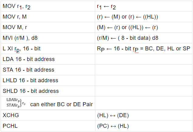
(iii) Arithmetic Instructions: This group consists of addition, subtraction, increment and decrement operations. 8085 microprocessor does not support multiplication and division instructionsADD r (A) ← (A)+ (A) ADD M (A) ← (A) + (M) ADl d8 (A) ← (A) + d8 ADC r (A) ← (A) + (r) + Cy ADC M (A) ← (A) + (M) + Cy ACI d8 (A) ← (A)+ d8 + Cy SUB r (A) ← (A) - (r) SUB M (A) ← (A) - (M) SUI d8 (A) ← (A) - d8 SBB r (A) ← (A) - (r) - Cy SBB M (A) ← (A) - (M) - Cy SBI d8 (A) ← (A) - d8 - Cy INR r (r) ← (r) + 1 INR M (M) ← (M) + 1 INX rp (rp) ← (rp) + 1 (rp = BC, DE, HL or SP) DCR r (r) ← (r) - 1 DCR M (M) ← (M) - 1 DCX rp (rp) ← (rp) - 1 (rp = BC, DE, HL or SP) DAD rP (HL) ← (HL) + (rp) (rp = BC, DE, HL or SP) DAA - In 8085, the service of AC flag is used by only one instruction. It is DAA.
- For INX and DCX instructions, no flags is affected
- Following table shows the list of flags affected for different instructions

(i) Logical Instructions: This group consists of AND, OR, NOT, XOR, Compare and Rotate operations
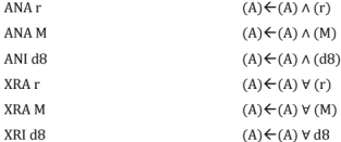
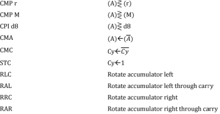
- Following table shows how flags affected for different logical instructions

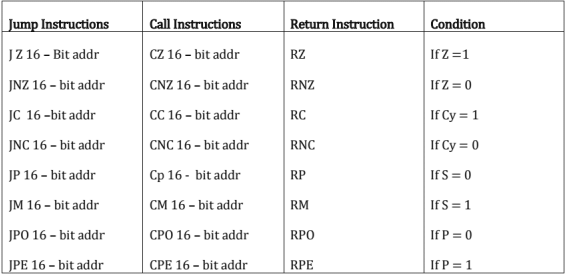
(i) Branch Instructions: These are also called program control transfer instruction. These are two types: Un conditional branch and Conditional branch instructions - No flags will be affected for branch instructions
- Unconditional Branch Instructions

- Conditional branch instruction
(i) Machine Control, Stack and 10 related Instructions: No Flags affected for these instructions. - Machine Control: El, DI, SIM, RIM, NOR HLT
- Stack related: PUSH rp (rp= BC<DE<HL)
PUSH PSW
POP rp
POP PSW
LXISP, 16-bitaddr
SPHL - 10 Related: IN 8 - IN 8 - bit Port address
OUT 8 - bit Port address - Whenever PUSH instruction is executed SP register content is decremented by 2.
- Whenever POP instruction is executed SP register content is incremented by 2.
- When CALL instruction (conditional or unconditional) or RST instruction is executed, SP register content is decremented by 2,
- When RET instruction (Conditional or Unconditional ) is executed, SP register content is incremented by 2, because it retrieves top two locations of the stack and load into PC
Addressing Modes: The way in which the operand information is specified in the instruction code is called addressing mode. The 8085 microprocessor supports five addressing modes.
- Implied or Implicit or Inherent Addressing Mode: There are certain instructions which operate on the content of the accumulator. Such instructions do not require the address of the operand. Eg: CMA, STC, RLC, RRC, RAL, RAR etc.
- Direct Addressing Mode: In this mode the address of the operand (data) is given in the instruction itself. Eg: STA, LDA, SHLD, LHLD, IN, OUT etc.
- Register Addressing Mode: In this mode the operands are in the general purpose registers. The operation code specifies the address of the register in addition to the operation to the performed. Eg: MOV A,B; ADDB; SUB C; ORA B ; etc.
- Register Indirect Addressing Mode; In this mode the address of the operand is specified by a register pair. Kg: LX1, STAZ, LDAX etc.
- Immediate Addressing Mode; In this mode the operand is specified in the instructions itself. Eg: MVL ADI, LX1, ORI, SU1, SBI, ACI, XR1,AN1 etc.
(i) Each instruction cycle of the 8085 microprocessor can be divided into a few basic operations called machine cycles, and each machine cycle can be divided into T-states.
(ii) Machine Cycle: It is defined as the time required completing the operation of accessing either memory or I/O. In the 8085, the machine cycle may consist of three to six T-states.
(iii) T-state is defined as one sub-division of the operation performed in one clock-period.
(iv) The time required to complete the execution of an instruction is called instruction cycle.
(v) The first machine cycle of 8085 consists of four to six T-states and all other subsequent machine cycles consist of three T-states only.
(vi) Types of machine cycle of 8085: Op code fetch cycle, memory read cycle, memory write cycle, I/O read cycle, I/O write cycle, Interrupt acknowledge machine cycle and Bus idle machine cycle.
(vii) The first machine cycle of each instruction cycle is always Op Code fetch machine cycle.
(viii) In 8085, CALL instruction is the lengthy instruction which takes 18-T states and the shortest instruction takes only 4-T states (Ex: MOV A,B)
(ix) Memory Mapping: Assigning address to memory locations is called memory mapping.
(x) Absolute Decoding: In this decoding all the address lines which are not used for memory chip to identify a memory register must be decoded.
(xi) Linear Decoding: In this decoding technique there is one address line for CS. This technique reduces hardware, but generates multiple addresses resulting in fold memory space.
(xii) I/O Devices Can be Connected to Microprocessor in Two Different Techniques.
1. Memory mapped I/O technique and
2. 1/0 mapped or peripheral mapped I/O technique
Memory Mapped I/O Technique
- In memory mapped I/O, the 1/0 devices are also treated as memory locations, under that assumption they will be given 16- bit address.
- In memory mapped I/O, microprocessor uses memory related instructions to communicate with I/O devices Eg: STA, LDA, MOV A,M; MOV B, M etc.
- In memory mapped I/O,
 control signals are used to activate I/O devices.
 - In memory mapped I/O the entire memory map is shared by memory locations and 1/0 devices one address can be used only once. This technique is used in a system where the number of I/O devices are less.
- The maximum numbers of I/O devices that can be connected to microprocessor in this technique are 65536.
I/O Mapped I/O Technique
- In this technique the I/O devices are identified by the microprocessor with separate 8-bit port address.
- This technique uses separate control signals
 to activate I/O devices and separate (IN and OUT) to communicate with I/O devices.
 - In the technique I/O mapping is independent of memory mapping, same address can be used to identify input device and output device.
- This technique is used in a system where number of I/O devices are more by using this method a maximum of 2S6 input devices and 256 output devices can be connected to the processor (total of 5121/0 devices).
|
1 videos|30 docs|57 tests
|


