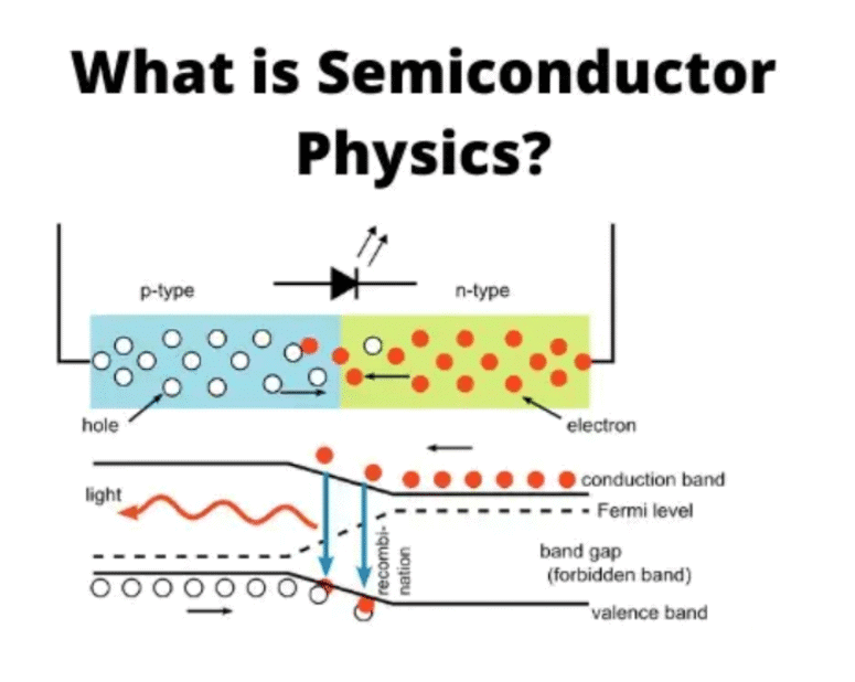
Semiconductor Physics | Solid State Physics, Devices & Electronics PDF Download
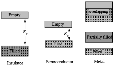
Metals, Semiconductors, and Insulators
- Every solid has its own unique energy band structure.
- The differences in band structure lead to a wide variety of electrical properties in different materials.
- For instance, the band structure of diamond helps explain why carbon in the diamond form is a good insulator.
- To understand this, we need to look at the characteristics of fully filled and completely empty energy bands during the process of conducting electricity.
- Before we dive deeper into how current flows in solids, we should note that for electrons to speed up in an electric field, they must be able to move to new energy states.
- This means there must be empty states (energy states that are not occupied by electrons) available for the electrons to move into.
- For example, if there are only a few electrons in an otherwise empty band, there are plenty of unoccupied states for the electrons to jump into.
- However, in the diamond structure, the valence band is completely filled with electrons at 0 K, and the conduction band is empty.
- This means there can be no charge movement within the valence band because there are no empty states for the electrons to occupy.
- Since the conduction band has no electrons, there can be no charge movement there either.
- Therefore, carbon in the diamond form has a high resistivity, which is typical for insulators.
- At 0 K, semiconductor materials have a similar structure to insulators, with a filled valence band and an empty conduction band separated by a band gap that has no allowed energy states.
- The key difference is the size of the band gap (Eg), which is much smaller in semiconductors than in insulators.
- For example, the semiconductor silicon has a band gap of about 1.1 eV, while diamond has a band gap of 5 eV.
- The smaller band gaps in semiconductors allow electrons to be excited from the lower (valence) band to the upper (conduction) band with reasonable amounts of thermal or optical energy.
- For instance, at room temperature, a semiconductor with a 1 eV band gap will have many electrons thermally excited into the conduction band, while an insulator with an Eg = 10 eV will have very few excitations.
- Thus, an important distinction between semiconductors and insulators is that the number of electrons available for conduction can significantly increase in semiconductors with added thermal or optical energy.
- In metals, the bands either overlap or are only partially filled.
- This means that electrons and empty energy states are mixed within the bands, allowing electrons to move freely when an electric field is applied.
- As expected from their band structures, metals exhibit high electrical conductivity.
 Direct and Indirect Semiconductors
- When calculating band structures, it is assumed that a single electron moves through a perfectly repeating lattice.
- The electron's wave function is considered to be a plane wave that travels in a specific direction, such as the x-direction, characterized by a propagation constant k, also known as a wave vector.
- The wave function of the electron varies in space and can be described as:
- U(kx, x) adjusts the wave function according to the periodic nature of the lattice.
- In these calculations, the possible energy values can be plotted against the propagation constant k.
- Since the repeating patterns of most lattices differ in various directions, the (E, k) diagram must be created for different crystal directions.
- The complete relationship between energy (E) and wave vector (k) forms a complex surface that is best represented in three dimensions.
- In the case of GaAs, the conduction band has a minimum energy point and the valence band has a maximum energy point at the same k value (k = 0).
- Conversely, for Si, the maximum energy point of the valence band occurs at a different k value than the minimum of the conduction band.
- Therefore, in GaAs, an electron can transition from the conduction band to the valence band with no change in k value, representing a direct transition.
- In contrast, a transition from the conduction band minimum to the valence band maximum in Si requires a change in k, which is known as an indirect transition.
- This indirect transition that involves a change in k also necessitates a change in the electron's momentum.
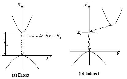
- In a direct semiconductor like GaAs, when an electron in the conduction band falls to an empty space in the valence band, it releases energy as a photon of light.
- Conversely, in an indirect semiconductor such as Si, an electron at the minimum of the conduction band cannot drop straight down to the maximum of the valence band.
- Instead, it must change both its momentum and its energy.
- For instance, the electron might pass through some defect state within the band gap (denoted as Et).
- In an indirect transition, which involves a change in k, the energy is usually released as heat to the lattice rather than as a photon.
- This distinction between direct and indirect band structures is crucial in determining which semiconductors can be used in devices that require light output.
- For example, devices that emit light, such as semiconductor light emitters and lasers, typically need to be made from materials that allow for direct band-to-band transitions or from indirect materials that enable vertical transitions between defect states.
Electrons and Holes
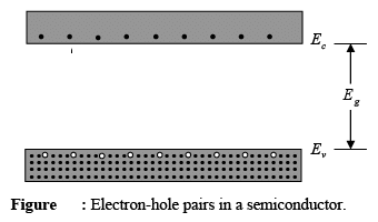
- As the temperature of a semiconductor increases from 0 K, some electrons in the valence band gain enough thermal energy to jump across the band gap into the conduction band.
- This leads to a situation where there are some electrons in the conduction band, which is usually empty, and there are also unfilled spots in the valence band, which is usually full.
- An unfilled spot in the valence band is called a hole.
- When an electron moves from the valence band to the conduction band, it creates both a conduction band electron and a hole.
- These two components—the electron and the hole—are known as an electron-hole pair, often shortened to EHP.
- When an electron gets enough energy to jump to the conduction band, it finds itself surrounded by many empty energy levels.
- In pure silicon (Si) at room temperature, the number of electron-hole pairs (EHP) is about 1010 EHP/cm3.
- This is very small compared to the density of silicon atoms, which is over 1022 atoms/cm3.
- Because there are only a few electrons in the conduction band, they can move freely through the many empty states available around them.

➤ Effective Mass
- The electrons within a crystal are not entirely free; instead, they interact with the periodic potential of the lattice structure.
- Because of this interaction, their wave-particle behavior cannot be expected to resemble that of electrons in open space.
- When we apply standard electrodynamics equations to charge carriers in solid materials, we need to adjust the values of the particle mass.
- This adjustment helps us to consider most of the effects of the lattice, allowing us to treat the electrons and holes as “almost free” carriers for most calculations.
- The calculation of effective mass must consider the shape of the energy bands in three-dimensional k-space.
- We also need to take appropriate averages across the different energy bands to ensure accuracy in our calculations.
Example 1: Find the ( E ,k) relationship for a free electron and relate it to the electron mass.
Solution: The electron momentum is p = . Then
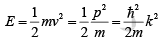
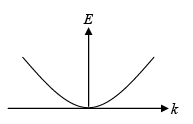
Thus the electron energy is parabolic with wave vector k .
 The electron mass is inversely related to the curvature (second derivative) of the ( E ,k) relationship, since
Although electrons in solids are not free, most energy bands are close to parabolic at their minima (for conduction bands) or maxima (for valence bands). We can also approximate effective mass near those band extrema from the curvature of the band.
The effective mass of an electron in a band with a given ( E ,k ) relationship is given by 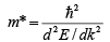
- A notable aspect is that the curvature d2E / dk2 is positive at the lowest points of the conduction band and negative at the highest points of the valence band.
- This means that electrons located near the top of the valence band have a negative effective mass.
- Electrons in the valence band, which carry a negative charge and have a negative mass, move in the same direction as holes that have a positive charge and positive mass when an electric field is applied.
- To fully understand how charge moves in the valence band, we can focus on how holes move.
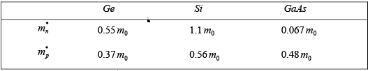
- When calculating the mass of charge carriers, it is important to use the effective mass values relevant to the specific material being studied.
- The table below shows the effective masses for Germanium (Ge), Silicon (Si), and Gallium Arsenide (GaAs) that are suitable for one type of calculation.
- In this table and in all future discussions, the effective mass of electrons is represented as mn*, while the effective mass of holes is represented as m*p.
- The n subscript indicates that electrons are negative charge carriers, and the p subscript indicates that holes are positive charge carriers.
- The rest mass of a free electron is noted as m0.
Intrinsic Material
- A perfect semiconductor crystal that has no impurities or defects is called an intrinsic semiconductor.
- In an intrinsic semiconductor at 0 Kelvin, there are no charge carriers because the valence band is completely filled with electrons and the conduction band is empty.
- When the temperature increases, electron-hole pairs (EHPs) are formed. This occurs when electrons in the valence band gain enough energy to jump across the energy gap (band gap) into the conduction band.
- The creation of EHPs can be understood by thinking about how covalent bonds in the crystal lattice break.
- If one of the silicon (Si) valence electrons breaks away from its bond, it becomes free to move. This creates a conduction electron and leaves behind a hole due to the broken bond.
- The energy needed to break this bond is known as the band gap energy (Eg).
- While this model helps to visualize how EHPs are formed, the energy band model is more useful for doing calculations.
- A key challenge with the "broken bond" model is that the free electron and the hole may seem to be fixed in location.
- In reality, the positions of the free electron and the hole are spread out over multiple lattice sites, and they should be understood using quantum mechanics through probability distributions.
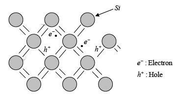
Electron-hole pairs in the covalent bonding model of the Si crystal
Since the electrons and holes are created in pairs, the conduction band electron concentration n (electrons per cm3) is equal to the concentration of holes in the valence band p (holes per cm3). Each of these intrinsic carrier concentrations is commonly referred to as ni. Thus for intrinsic material, n = p = ni.
At a given temperature there is a certain concentration of electron-hole pairs ni . Obviously, if a steady state carrier concentration is maintained, there must be recombination of EHPs at the same rate at which they are generated. Recombination occurs when an electron in the conduction band makes a transition (direct or indirect) to an empty state (hole) in the valence band, thus annihilating the pair. If we denote the generation rate of EHPs as gi, (EHP/cm3) and the recombination rate as ri , equilibrium requires that:
ri =gi
Each of these rates is temperature dependent. For example, gi (T ) increases when the temperature is raised, and a new carrier concentration ni , is established such that the higher recombination rate ri (T) just balances generation. At any temperature, we can predict that the rate of recombination of electrons and holes ri is proportional to the equilibrium concentration of electrons n0 and the concentration of holes p0
The factor αr is a constant of proportionality which depends on the particular mechanism by which recombination takes place.
Extrinsic Material
- In addition to the carriers created by heat, it is also possible to create carriers in semiconductors intentionally by adding impurities to the crystal.
- This process, known as doping, is a common method for changing the conductivity of semiconductors.
- Doping modifies a crystal so that it has more electrons or holes.
- There are two main types of doped semiconductors:
- n-type: mostly contains electrons
- p-type: mostly contains holes
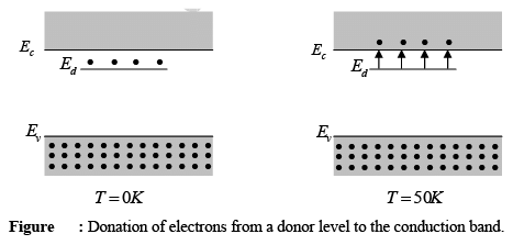
- When impurities or defects are added to a perfect crystal, they create extra energy levels in the energy band structure, typically within the band gap.
- For example, an impurity from group V of the periodic table (like P, As, and Sb) adds an energy level close to the conduction band in germanium (Ge) or silicon (Si).
- This level is filled with electrons at absolute zero (0 K), and only a small amount of thermal energy is needed to move these electrons to the conduction band.
- By around 50 K to 100 K, nearly all electrons in the impurity level can be excited into the conduction band.
- The impurity level that allows this is referred to as a donor level, and the group V impurities in Ge or Si are called donor impurities.
- It is noted that materials doped with donor impurities can have a high concentration of electrons in the conduction band, even when the temperature is too low for the naturally occurring electron-hole pair (EHP) concentration to be significant.
- Therefore, semiconductors with many donor atoms will have a concentration of electrons (n0) much greater than the intrinsic concentration (ni) and hole concentration (p0) at room temperature, indicating that this is an n-type material.
Atoms from column III (B, Al, Ga, and In) introduce impurity levels in Ge or Si near the valence band. These levels are empty of electrons at 0 K . At low temperatures, enough thermal energy is available to excite electrons from the valence band into the impurity level, leaving behind holes in the valence band, since this type of impurity level “accepts” electrons from the valence band, it is called an acceptor level, and the column III impurities are acceptor impurities in Ge and Si. Figure indicates, doping with acceptor impurities can create a semiconductor with a hole concentration p0 much greater than the conduction band electron concentration n0 (this is p-type material).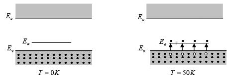 Acceptance of valence band electrons by an acceptor level, and the resulting creation of holes.
The Fermi Level
Electrons in solids obey Fermi-Dirac statistics. In the development of this type of statistics, one must consider the indistinguishability of the electrons, their wave nature, and the Pauli Exclusion Principle. The rather simple result of these statistical arguments is that the distribution of electrons over a range of allowed energy levels at thermal equilibrium is:
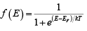
where k is Boltzmann constant. The function f (E), the Fermi-Dirac distribution function, gives the probability that an available energy state at E will be occupied by an electron at absolute temperature T. The quantity EF is called the Fermi Level, and it represents an important quantity in the analysis of semiconductor behavior. We notice that, for an energy E equal to the Fermi level energy EF, the occupation probability is 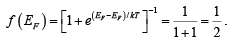
A closer examination of f (E) indicates that at 0 K the distribution takes the simple rectangular form shown in figure. With T = 0 in the denominator of the exponent, f ( E ) is 1/(1 + 0) = 1 when the exponent is negative (E < EF), and is 1/ (1 + ∞) = 0 when the exponent is positive (E > EF). This rectangular distribution implies that at 0 K every available energy state up to EF is filled with electrons and all states above EF are empty.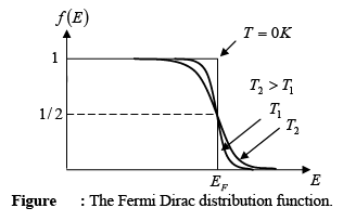
At temperatures higher than 0 K , some probability exists for states above EF to be filled. For example, at T =T1 there is some probability f (E) that states above EF are filled, and there is a corresponding probability [1 − f (E)] that states below EF are empty.
- The Fermi function is symmetrical around EF at all temperatures. This means that the chance f(EF + ΔE) of a state ΔE above EF being occupied is equal to the chance [1 - f(EF - ΔE)] that a state ΔE below EF is unoccupied.
- This symmetry of filled and unfilled states around EF makes it a useful reference point when calculating the amounts of electrons and holes in semiconductors.
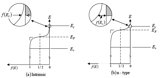
- For intrinsic materials, the number of holes in the valence band is the same as the number of electrons in the conduction band. Therefore, the Fermi level (EF) is positioned in the middle of the band gap.
- Since f(E) is symmetrical around EF, the part of the function that shows the probability of finding electrons in the conduction band is balanced by the part showing holes in the valence band.
- Within the band gap, between Ec and Ev, there are no available energy states. As a result, the function f(E) does not indicate any electron occupancy in this area.
- In n-type materials, there is a greater number of electrons in the conduction band compared to holes in the valence band. Thus, the distribution function f(E) is positioned higher than it would be in an intrinsic material.
- Since the shape of f(E) stays the same for a specific temperature, a larger number of electrons at Ec in n-type materials leads to a smaller number of holes at Ev.
- As the Fermi level (EF) moves closer to Ec, the value of f(E) for each energy level in the conduction band—and thus the total electron concentration (n0)—increases. The energy difference (Ec - EF) indicates the number of electrons.
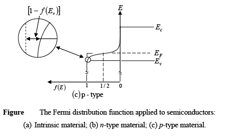
- For p-type materials, the Fermi level is closer to the valence band, making the [1 - f(E)] tail below Ev larger than the f(E) tail above Ec.
- The difference (EF - Ev) shows how strongly the material behaves as p-type.
- Instead of drawing the function f(E) versus E on every energy band diagram to show the distribution of electrons and holes, it is common to simply mark the position of EF on the diagrams.
 |
Download the notes
Semiconductor Physics
|
Download as PDF |
➤ Electron and Hole Concentrations at Equilibrium
The Fermi distribution function can be used to calculate the concentrations of electrons and holes in a semiconductor, if the densities of available states in the valence and conduction bands are known. For example, the concentration of electrons in the conduction band is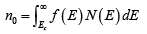
where N (E) dE is the density of states (cm-3) in the energy range dE . The subscript 0 used with the electron and hole concentration symbols (n0, p0) indicates equilibrium conditions. The number of electrons per unit volume in the energy range dE is the product of the density of states and the probability of occupancy f ( E ) . Thus the total electron concentration is the integral over the entire conduction band. The function N (E) can be calculated by using quantum mechanics and the Pauli Exclusion Principle.
Since N (E) is proportional to E1/ 2 , so the density of states in the conduction band increases with electron energy. On the other hand, the Fermi function becomes extremely small for large energies. The result is that the product f (E)N(E) decreases rapidly above Ec and very few electrons occupy energy states far above the conduction band edge. Similarly, the probability of finding an empty state (hole) in the valence band [1 − f(E)] decreases rapidly below Ev and most holes occupy states near the top of the valence band. This effect is demonstrated, which shows the density of available states, the Fermi function, and the resulting number of electrons and holes occupying available energy states in the conduction and valence bands at thermal equilibrium (i.e., with no excitations except thermal energy). For holes, increasing energy points down, since the E scale refers to electron energy.
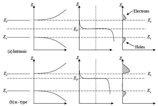
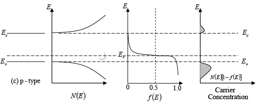
Figure : Schematic band diagram, density of states, Fermi-Dirac distribution, and the carrier concentrations for (a) intrinsic, (b) n-type, and (c) p-type semiconductors at thermal equilibrium.
The result of the integration of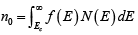 is the same as that obtained if we represent the entire distributed electron states in the conduction band by an effective density of states Nc located at the conduction band edge Ec . Therefore, the conduction band electron concentration is simply the effective density of states at Ec times the probability of occupancy at Ec
n0 =f (Ec) Nc
In this expression we assume the Fermi level EF lies at least several kT below the conduction band. Then the exponential term is large compared with unity and the Fermi function f(Ec) can be simplified as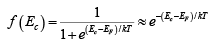
Since kT at room temperature is only 0.026 eV , this is generally a good approximation. For this condition the concentration of electrons in the conduction band is 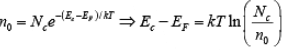
The effective density of states 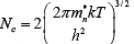
Thus electron concentration increases as EF moves closer to the conduction band. By similar arguments, the concentration of holes in the valence band is p0 = N[1 −f(Ev)]
where Nc is the effective density of states in the valence band.
The probability of finding an empty state at Ev is, 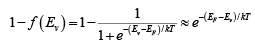 for EF larger than Ev by several kT.
From these equations, the concentration of holes in the valence band is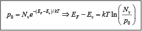
The effective density of states in the valence band 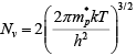
Thus hole concentration increases as EF moves closer to the valence band.
The electron and hole concentrations predicted by above equations are valid whether the material is intrinsic or doped, provided thermal equilibrium is maintained.
Thus for intrinsic material, EF lies, at some intrinsic level Ei near the middle of the band gap, and the intrinsic electron and hole concentrations are 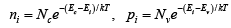
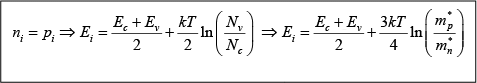
Note: The intrinsic level Ei is the middle of the band gap  if the effective densities of states Nc and Nc are equal. There is usually some difference in effective mass for electrons and holes, however, and Nc and Nc are slightly different.
The product of n0 and p0 at equilibrium is a constant for a particular material and temperature, even if the doping is varied: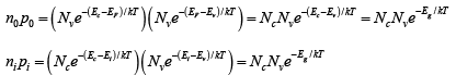
The intrinsic electron and hole concentrations are equal (since the carriers are created in pairs), ni =pi ; thus the intrinsic concentration is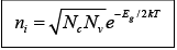
Law of Mass Action
The constant product of electron and hole concentrations can be written conveniently as 
For n-type material the minority concentration (holes)  where ND is donor ion concentration.
For p-type material the minority concentration (electrons)  where NA is acceptor ion concentration.
Another convenient way of writing electron and hole concentration is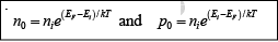
This form of the equation indicates directly that the electron concentration is ni when EF is at the intrinsic level Ei and that n0 increases exponentially as the Fermi level moves away from Ei toward the conduction band. Similarly, the hole concentration p0 varies from ni to larger values as EF moves from Ei, toward the valence band. Since these equations reveal the qualitative features of carrier concentration so directly, they are particularly convenient to remember.
 |
Take a Practice Test
Test yourself on topics from Physics exam
|
Practice Now |
Temperature Dependence of Carrier Concentrations
The variation of carrier concentration with temperature is indicated by equations . Initially, the variation of n0 and p0 with T seems relatively straightforward in these relations. The problem is complicated, however, by the fact that ni has strong temperature dependence
  and that FE can also vary with temperature. Let us begin by examining the intrinsic carrier concentration.
The exponential temperature dependence dominates ni(T) and a plot of ln (ni) vs 1000/T appears almost linear. 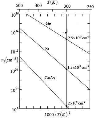 Intrinsic carrier concentration for Ge, Si, and GaAs as a function of inverse temperature. The room temperature values are marked for reference
Compensation and Space Charge Neutrality
- The figure shows a semiconductor that has both donors and acceptors, but with more donors than acceptors (ND > NA).
- Because there are more donors, the semiconductor is classified as n-type, and the Fermi level is located in the upper part of the band gap.
- The Fermi level (EF) is much higher than the acceptor level (Ea), which means that the acceptor levels are mostly filled with electrons.
- Since EF is positioned above the intrinsic level (Ei), we cannot expect the number of holes in the valence band to match the number of acceptors.
- Essentially, the filling of the Ea states uses up the electrons donated to the conduction band.
- The process can be explained like this:
- When an acceptor state gets filled with an electron from the valence band, it creates a hole in the valence band.
- This hole is then filled by an electron from the conduction band, leading to a decrease in the number of electrons in the conduction band.
- If we apply this idea to all the acceptor atoms, the number of electrons left in the conduction band will be ND - NA instead of just ND.
- This situation is referred to as compensation.
- Through this compensation, we can start with an n-type semiconductor and add acceptors until the number of acceptors equals the number of donors (NA = ND).
- At this point, there will be no donated electrons left in the conduction band, resulting in n0 = ni = p0, which allows for intrinsic conduction.
- If we continue to add more acceptors, the semiconductor will change to p-type, with a hole concentration that is essentially NA - ND.
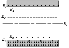 Compensation in an n-type semiconductor (ND > NA)
The exact relationship among the electron, hole, donor, and acceptor concentrations can be obtained by considering the requirements for space charge neutrality. If the material is to remain electrostatically neutral, the sum of the positive charges (holes and ionized donor atoms) must balance the sum of the negative charges (electrons and ionized acceptor atoms): 
Thus the net electron concentration in the conduction band is 
If the material is doped n-type ( n0 >>p0) and all the impurities are ionized, we can approximate that n0 = ND − NA .
Since the intrinsic semiconductor itself is electrostatically neutral and the doping atoms we add are also neutral, the requirement of equation  must be maintained at equilibrium.
Knowledge of carrier concentrations in a solid is necessary for calculating current flow in the presence of electric or magnetic fields. In addition to the values of n and p, we must be able to take into account the collisions of the charge carriers with the lattice and with the impurities. These processes will affect the ease with which electrons and holes can flow through the crystal, that is, their mobility within the solid. As should be expected, these collision and scattering processes depend on temperature, which affects the thermal motion of the lattice atoms and the velocity of the carriers.
Example 2: The donor concentration in a sample of n -type silicon is increased by a factor of 100. Find the shift in the position of the Fermi level at 300 K . (kBT = 25 meV at 300K)
Solution:
Thus shift is ΔE= kT ln (100) = 25 ln (100 ) meV = 115.15 meV

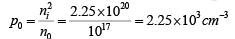
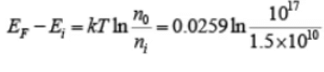
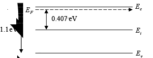
Example 3: A Si sample is doped with 1017 As atoms/cm3. What is the equilibrium hole concentration p0 at 300 K? Where is EF relative to Ei (where ni = 1.5×1010cm−3)
Solution: Since ND >> ni we can approximate ni and
= 0.407 eV
|
91 videos|21 docs|25 tests
|
FAQs on Semiconductor Physics - Solid State Physics, Devices & Electronics
| 1. What is effective mass in semiconductor physics? |  |
| 2. How does effective mass affect the electrical conductivity of semiconductors? | |
| 3. What factors influence the effective mass of charge carriers in a semiconductor? | |
| 4. How can effective mass be experimentally determined in semiconductors? | |
| 5. Why is the concept of effective mass important for semiconductor device engineering? | |


Semester Notes
,Exam
,MCQs
,video lectures
,Extra Questions
,shortcuts and tricks
,Sample Paper
,Devices & Electronics
,Semiconductor Physics | Solid State Physics
,Semiconductor Physics | Solid State Physics
,practice quizzes
,Semiconductor Physics | Solid State Physics
,study material
,Previous Year Questions with Solutions
,Summary
,Free
,Important questions
,ppt
,past year papers
,Viva Questions
,mock tests for examination
,Devices & Electronics
,Devices & Electronics
,Objective type Questions
;


Semiconductor Physics Free PDF Download
Importance of Semiconductor Physics
Semiconductor Physics Notes
Semiconductor Physics Physics Questions
Study Semiconductor Physics on the App
|
© EduRev
|
Education Revolution
|


|


within 7 days!