Q21: A 1 : 1 Pulse Transformer (PT) is used to trigger the SCR in the below figure. The SCR is rated at 1.5 kV, 250 A with IL = 250 mA, IH = 150 mA, and IGmax = 150 mA, IGmin = 100 mA. The SCR is connected to an inductive load, where L = 150 mH in series with a small resistance and the supply voltage is 200 V dc. The forward drops of all transistors/diodes and gate-cathode junction during ON state are 1.0 V
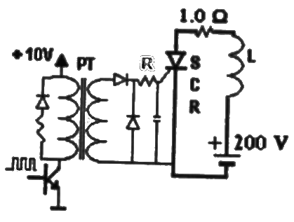 The resistance R should be (2007)
(a) 4.7kΩ
(b) 470kΩ
(c) 47Ω
(d) 4.7Ω
Ans: (c)
Sol: 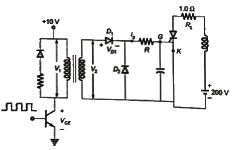 When the pulses are applied to the base of the transistor. Transistor operates in ON state. So, the forward voltage drop in trnasistor VCE = 1V.
 D1 is forward baised and voltage drop in diode VD1 = 1V.
D2 is reversed biasesd and acts as open circuit. Capacitor behaves as open circuit for dc voltage.
Forward voltage drop of gate cathode junction Vgk = 1V
Voltage drop across resistor R,
 To ensure turn -ON of SCR

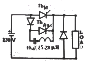
Q22: The circuit in the figure is a current commutated dc-dc chopper where, ThM is the main SCR and ThAUX is the auxiliary SCR. The load current is constant at 10 A. ThM is ON. ThAUX is trigged at t = 0. ThM is turned OFF between. (2007)
 (a) 0μs < t ≤ 25μs
(b) 25μs < t ≤ 50μs
(c) 50μs < t ≤ 75μs
(d) 75μs < t ≤ 100μs
Ans: (c)
Sol: 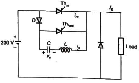 At t = 0−, vc = Vs, ic = 0 and iT1 = I0
At t = 0, Thaux is triggered, a resonant current ic designs to flow from C through Thaux, L and back to C.
This resonant current is given by
 after half a cycle of
  As ic tends to reverse, Thaux is turned off.
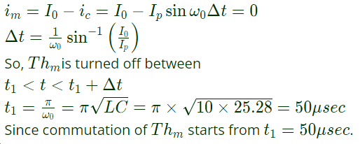
When vc = −Vs right hand plate has positive polarity, resonant current ic now builds up through C, L, D and Thm. As this current ic grows opposite to forward thyristor current of Thm, net forward current im = I0 − ic begins to decrease. Finaly when ic in the reversed direction attains the value I0, im is reduced to zero and Thm is turned off.
Q23: In the circuit of adjacent figure the diode connects the ac source to a pure inductance L.
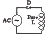 The diode conducts for (2007)
(a) 90°
(b) 180°
(c) 270°
(d) 360°
Ans: (d)
Sol: 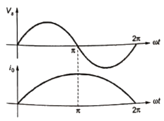
 Diode conducts for 360°.
Q24: An SCR having a turn ON times of 5 μsec, latching current of 50 mA and holding current of 40 mA is triggered by a short duration pulse and is used in the circuit shown in figure. The minimum pulse width required to turn the SCR ON will be (2006)
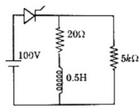 (a) 251 μsec
(b) 150 μsec
(c) 100 μsec
(d) 5 μsec
Ans: (b)
Sol: 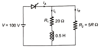 Current through 5kΩ resistor,
 Current through inductor,
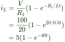 Anode current,
Ia = iR + iL = 0.02+5(1−e−40t)
Let minimum pulse width is T
To turn on ia ≥ latching current
⇒ 0.02 + 5(1 − e−40t) = 50mA = 0.5
T = 150 μsec
Q25: A voltage commutation circuit is shown in figure. If the turn-off time of the SCR is 50 μsec and a safety margin of 2 is considered, then what will be the approximate minimum value of capacitor required for proper commutation ? (2006)
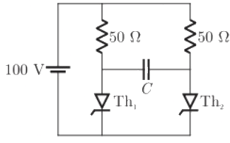 (a) 2.88 μF
(b) 1.44 μF
(c) 0.91 μF
(d) 0.72 μF
Ans: (a)
Sol: 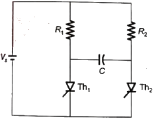 In this type of commutation, athyristor carrying load current is commutated by transferring its load current to another incoming thyristor.
Firing of SCR Th1 commutates Th2 and subsequently, firing of SCR Th2 would turn-off Th1.
Circuit turn-off time tc1 for Th1
tc1 = R1C ln 2
and circuit turn-off time tc2 for Th2
 Safety margin = 2

Q26: An electronics switch S is required to block voltage of either polarity during its OFF state as shown in the figure (a). This switch is required to conduct in only one direction its ON state as shown in the figure (b)
 Which of the following are valid realizations of the switch S? (2005)
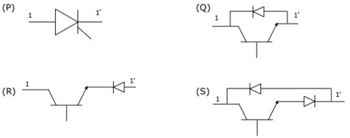 (a) Only P
(b) P and Q
(c) P and R
(d) R and S
Ans: (c)
Sol:  1: Switch s blocks voltage of both polarity, it means s can block forward as well as reverse voltage.
 2: Current through s, flows in forward direction only.
 Thyristor blocks voltage in either polarity until gate is triggered. Once the thyristor is triggered current flows in forward direction.
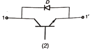
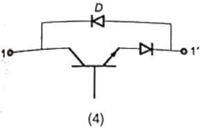 when the reverse voltage is applied across the device (2) and (4), current flows through diode indicated with D. So, these device do not satisfy the requirement.
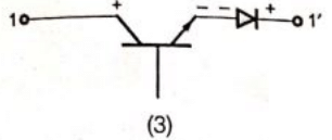 Transistor blocks positive voltage and diode blocks, negative voltage. Once the basae signal is applied, the device conducts in forward direction.
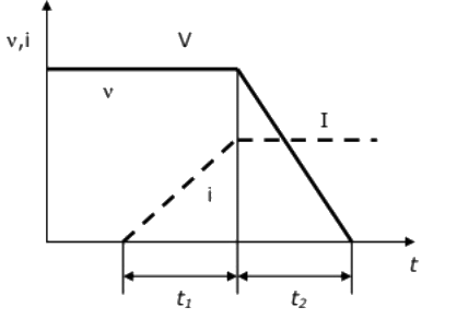
Q27: The figure shows the voltage across a power semiconductor device and the current through the device during a switching transitions. Is the transition a turn ON transition or a turn OFF transition ? What is the energy lost during the transition ? (2005)
 (a) Turn ON, (VI/2) (t1 + t2)
(b) Turn OFF, VI (t1+t2)
(c) Turn ON, VI (t1+t2)
(d) Turn OFF, (VI/2) (t1 + t2)
Ans: (a)
Sol: During interval t2, voltage starts decreasing and becomes zero and current starts increasing and becomes constant (I), so transition is turn on.
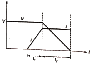 During t1 interval:
Power loss = vi
E1 = Energy loss = ∫vi dt = V∫i dt
V is constant during this period v = V
∫i dt represents area under i - t curve
 During t2 interval:
Power loss = vi
E2 = Energy loss = ∫vi dt = I ∫ v dt
i is constant during this period i = I
∫v dt represents area under v - t curve
 Total energy lost during the transition

Q28: The conduction loss versus device current characteristic of a power MOSFET is best approximated by (2005)
(a) a parabola
(b) a straight line
(c) a rectangular hyperbola
(d) an exponentially decaying function
Ans: (a)
Sol: Let, I = device current
RON = ON state resistance of power MOSFET
Conduction loss = P = I2RON
Therefore, condition losses versus device current characteristics can be best approximated by a parabola.
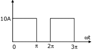
Q29: A MOSFET rated for 15 A, carries a periodic current as shown in figure. The ON state resistance of the MOSFET is 0.15 Ω. The average ON state loss in the MOSFET is (2004)
 (a) 33.8 W
(b) 15.0 W
(c) 7.5 W
(d) 3.8 W
Ans: (c)
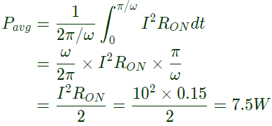
Sol: Rated current during on state I = 10
ON state resistance RON = 0.15Ω
MOSFET is ON
 MOSFET is OFF
 Average ON state Loss,
Q30: A bipolar junction transistor (BJT) is used as a power control switch by biasing it in the cut-off region (OFF state) or in the saturation region (ON state). In the ON state, for the BJT (2004)
(a) both the base-emitter and base-collector junctions are reverse biased
(b) the base-emitter junction is reverse biased, and the base-collector junction is forward biased
(c) the base-emitter junction is forward biased, and the base-collector junction is reverse biased
(d) both the base-emitter and base-collector junctions are forward biased
Ans: (d)
Sol: VCB = VCE − VDE...(i)
Under saturated state, VBES is greater than VCES this means base -emitter junction (BES) is forward baised. Further eq, (i) shows that VCB is negative under saturated conditions, therefore base-collector junction (CBJ) is also forward baised.
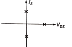
Q31: Figure shows a MOSFET with an integral body diode. It is employed as a power switching device in the ON and OFF states through appropriate control. The ON and OFF states of the switch are given on the VDS - IS plane by (2003)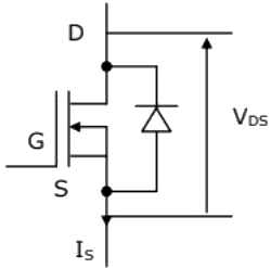 (a)
(a) 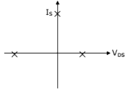 (b)
(b) 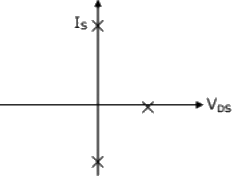 (c)
(c) 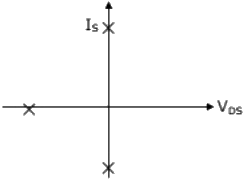 (d)
(d) 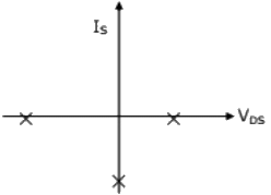 Ans: (b)
Sol:
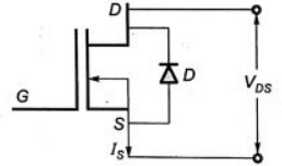
when reverse current flow through diode D.
So IS < 0 and VDS = 0
When MOSFET is in ON state
IS > 0 and VDS = 0
When MOSFET is in OFF state
IS = 0 and VDS > 0
Q32: Figure shows a thyristor with the standard terminations of anode (A), cathode (K), gate (G) and the different junctions named J1, J2 and J3. When the thyristor is turned on and conducting (2003)
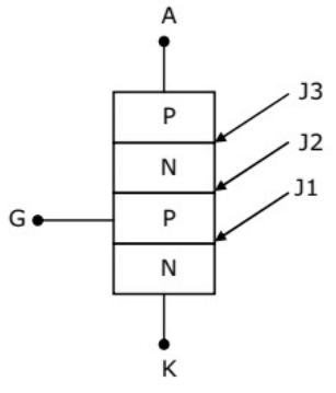 (a) J1 and J2 are forward biased and J3 is reverse biased
(b) J1 and J3 are forward biased and J2 is reverse biased
(c) J1 is forward biased and J2 and J3 are reverse biased
(d) J1, J2 and J3 are all forward biased
Ans: (d)
Q33: The main reason for connecting a pulse transformer at the output stage of a thyristor triggering circuit is to (2001)
(a) amplifying the power of the triggering pulse
(b) provide electrical isolation
(c) reduce the turn on time of the thyristor
(d) avoid spurious triggering of the thyristor due to noise
Ans: (b)
 The resistance R should be (2007)
 When the pulses are applied to the base of the transistor. Transistor operates in ON state. So, the forward voltage drop in trnasistor VCE = 1V.
 D1 is forward baised and voltage drop in diode VD1 = 1V.
 To ensure turn -ON of SCR
 (a) 0μs < t ≤ 25μs
 At t = 0−, vc = Vs, ic = 0 and iT1 = I0
 after half a cycle of
  As ic tends to reverse, Thaux is turned off.
 The diode conducts for (2007)
 Diode conducts for 360°.
 (a) 251 μsec
 Current through 5kΩ resistor,
 Current through inductor,
 Anode current,
 (a) 2.88 μF
 In this type of commutation, athyristor carrying load current is commutated by transferring its load current to another incoming thyristor.
 Safety margin = 2
 Which of the following are valid realizations of the switch S? (2005)
 (a) Only P
 1: Switch s blocks voltage of both polarity, it means s can block forward as well as reverse voltage.
 2: Current through s, flows in forward direction only.
 Thyristor blocks voltage in either polarity until gate is triggered. Once the thyristor is triggered current flows in forward direction.
 when the reverse voltage is applied across the device (2) and (4), current flows through diode indicated with D. So, these device do not satisfy the requirement.
 Transistor blocks positive voltage and diode blocks, negative voltage. Once the basae signal is applied, the device conducts in forward direction.
 (a) Turn ON, (VI/2) (t1 + t2)
 During t1 interval:
 During t2 interval:
 Total energy lost during the transition
 (a) 33.8 W
 MOSFET is OFF
 Average ON state Loss,
 (a)
(a)  (b)
(b)  (c)
(c)  (d)
(d)  Ans: (b)

 (a) J1 and J2 are forward biased and J3 is reverse biased


