Electrical Engineering (EE) Exam > Electrical Engineering (EE) Notes > Analog and Digital Electronics > Field Effect Transistor
Field Effect Transistor | Analog and Digital Electronics - Electrical Engineering (EE) PDF Download
Introduction
- The Field effect transistor abbreviated as FET , is an another semiconductor device like a BJT which can be used as an amplifier or a switch.
- The Field effect transistor is a voltage operated device. Whereas Bipolar junction transistor is a current controlled device. Unlike BJT a FET requires virtually no input current.
- This gives it an extremely high input resistance, which is its most important advantage over a bipolar transistor.
- FET is also a three-terminal device, labelled as source, drain and gate.
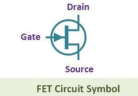
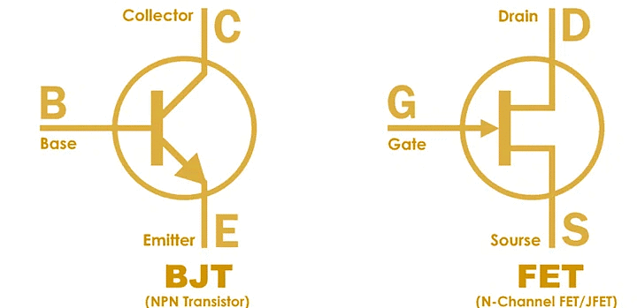
- The source can be viewed as BJT’s emitter, the drain as collector, and the gate as the counter part of the base.
- The material that connects the source to drain is referred to as the channel.
- FET operation depends only on the flow of majority carriers; therefore they are called uni polar devices. BJT operation depends on both minority and majority carriers.Question for Field Effect TransistorTry yourself:Which one is a unipolar device?View Solution
- As FET has conduction through only majority carriers it is less noisy than BJT.
- FETs are much easier to fabricate and are particularly suitable for ICs because they occupy less space than BJTs.
- FET amplifiers have low gain bandwidth product due to the junction capacitive effects and produce more signal distortion except for small signal operation.
- The performance of FET is relatively unaffected by ambient temperature changes. As it has a negative temperature coefficient at high current levels, it prevents the FET from thermal breakdown. The BJT has a positive temperature coefficient at high current levels which leads to thermal breakdown.
Question for Field Effect TransistorTry yourself:How many terminals does the FET transistor have?
View Solution
Classification of FET
There are two major categories of field effect transistors:
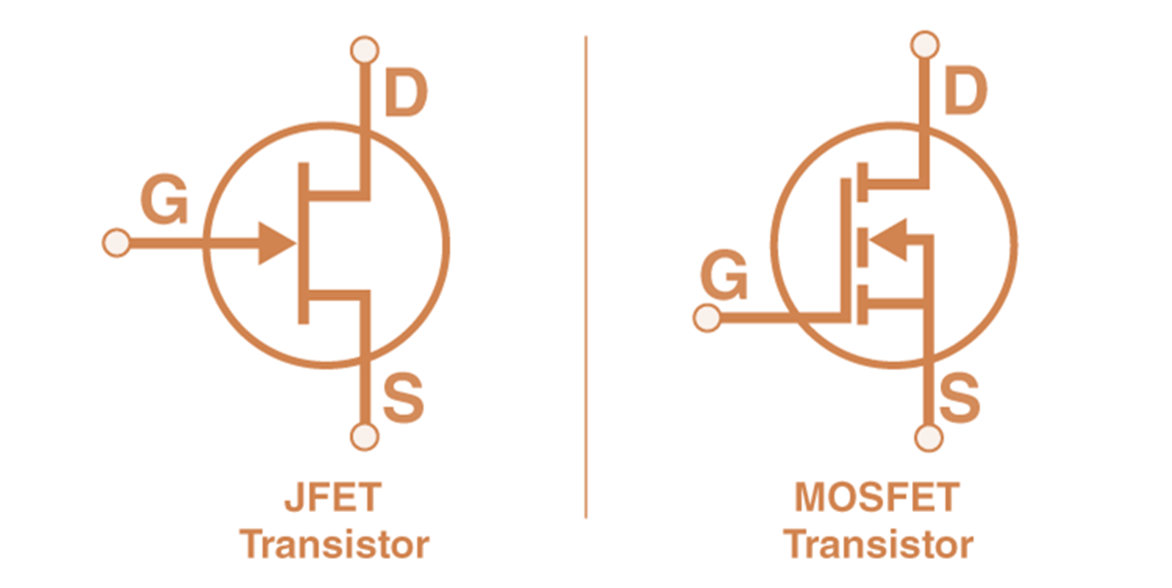
- Junction Field Effect Transistors (JFET)
- MOSFETs
These are further sub-divided into P- channel and N-channel devices.
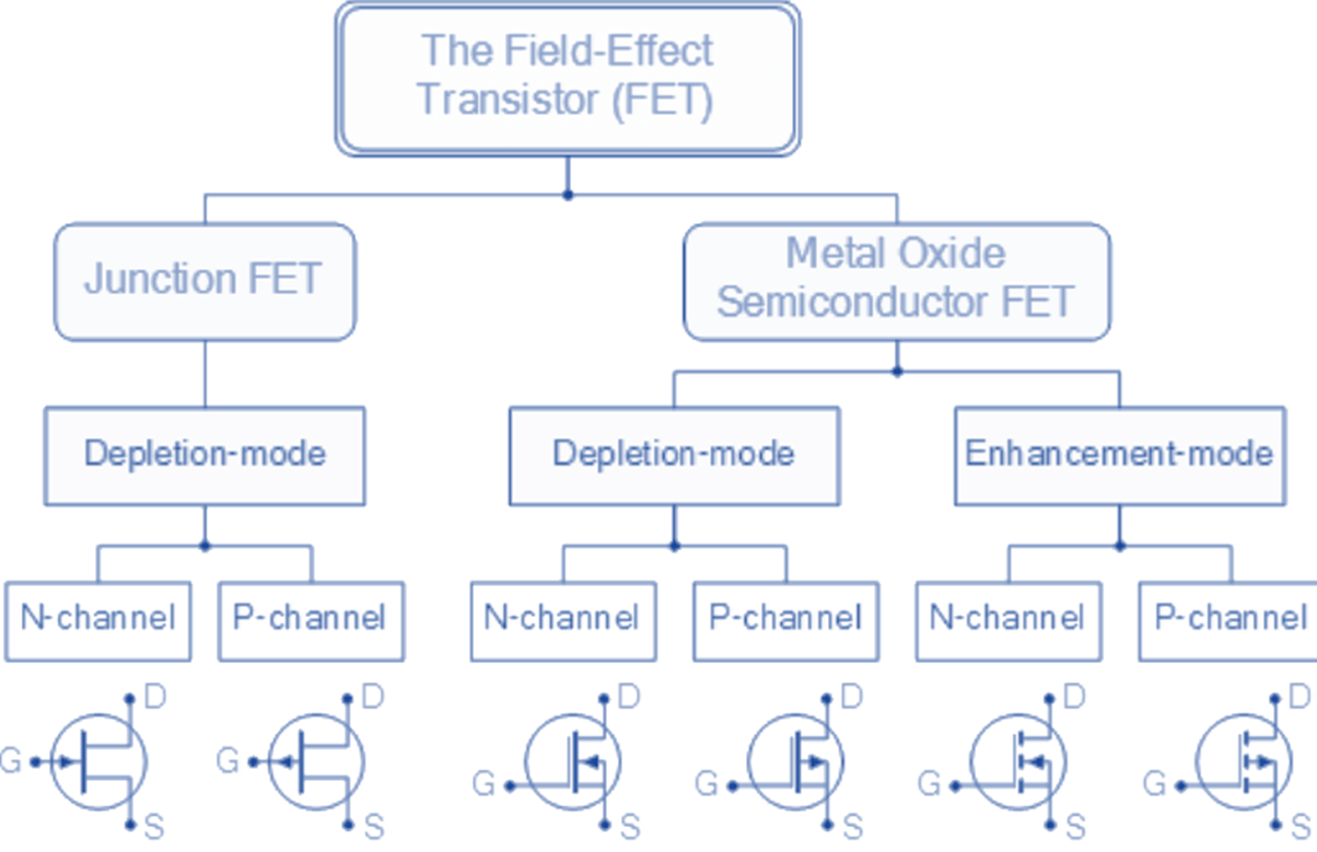
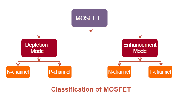
MOSFETs are further classified into two types:
- Depletion MOSFETs
- Enhancement MOSFETs.
When the channel is of N-type the JFET is referred to as an N-channel JFET, when the channel is of P-type the JFET is referred to as P-channel JFET. The schematic symbols for the P-channel and N-channel JFETs are shown in the figure.
Question for Field Effect TransistorTry yourself:How many types of MOSFETs are there?
View Solution
Construction & Operation of N- Channel FET
(i) Construction of N- Channel JFET
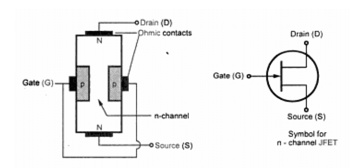
- A piece of N- type material, referred to as channel has two smaller pieces of P-type material attached to its sides, forming PN Junctions.
- The channel ends are designated as the drain and source . And the two pieces of P-type material are connected together and their terminal is called the gate.
- Since this channel is in the N-type bar, the FET is known as N-channel JFET.
(ii) Operation of N- Channel JFET
- The overall operation of the JFET is based on varying the width of the channel to control the drain current.
- A piece of N-type material referred to as the channel, has two smaller pieces of P-type material attached to its sites, forming PN-Junctions.
- The channel’s ends are designated the drain and the source. And the two pieces of P-type material are connected together and their terminal is called the gate.
- With the gate terminal not connected and the potential applied positive at the drain and negative at the source, a drain current Id flows.
- When the gate is biased negative with respect to the source, the PN junctions are reverse biased and depletion regions are formed. The channel is more lightly doped than the P-type gate blocks, so the depletion regions penetrate deeply into the channel.
- Since depletion region is a region with less no. of charge carriers so it behaves as an insulator. The result is that the channel is narrowed. Its resistance is increased, and Id is reduced.
- When the negative gate bias voltage is further increased, the depletion regions meet at the center and Id is cut off completely.
There are two ways to control the channel width
- By varying the value of Vgs
- By Varying the value of Vds holding Vgs constant
1. By Varying the Value of Vgs
- We can vary the width of the channel and in turn vary the amount of drain current. This can be done by varying the value of Vgs. This point is illustrated in the fig below.
- Here we are dealing with N-channel FET. So channel is of N-type and gate is of P-type that constitutes a PN junction. This PN junction is always reverse biased in JFET operation.
- The reverse bias is applied by a battery voltage Vgs connected between the gate and the source terminal i.e positive terminal of the battery is connected to the source and negative terminal to gate.
- When a PN junction is reverse biased the electrons and holes diffuse across junction by leaving immobile ions on the N and P sides , the region containing these immobile ions is known as depletion region.
- If both P and N regions are heavily doped then the depletion region extends symmetrically on both sides.
- But in N-channel FET P region is heavily doped than N-type thus depletion region extends more in N region than P region.
- So when no Vds is applied the depletion region is symmetrical and the conductivity becomes zero. Since there are no mobile carriers in the junction.
- As the reverse bias voltage increases the thickness of the depletion region also increases. i.e. the effective channel width decreases .
- By varying the value of Vgs we can vary the width of the channel.
2. Varying the value of Vds holding Vgs constant
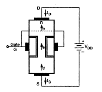 n-channel JFET with gate open & VDD applied between drain and source
- When no voltage is applied to the gate i.e. Vgs=0 , Vds is applied between source and drain the electrons will flow from source to drain through the channel constituting drain current Id .
- With Vgs= 0 for Id= 0, the channel between the gate junctions is entirely open. In response to a small applied voltage Vds , the entire bar acts as a simple semi-conductor resistor and the current Id increases linearly with Vds .
- The channel resistances are represented as rd and rs as shown in the fig above.
- This increasing drain current Id produces a voltage drop across rd which reverse biases the gate to source junction,(rd> rs). Thus the depletion region is formed which is not symmetrical .
- The depletion region developed penetrates deeper into the channel near drain and less towards source because Vrd >> Vrs. So reverse bias is higher near drain than at source.
- As a result, growing depletion region reduces the effective width of the channel. Eventually a voltage Vds is reached at which the channel is pinched off. This is the voltage where the current Id begins to level off and approach a constant value.
- So, by varying the value of Vds we can vary the width of the channel holding Vgs constant.
When both Vgs and Vds is applied
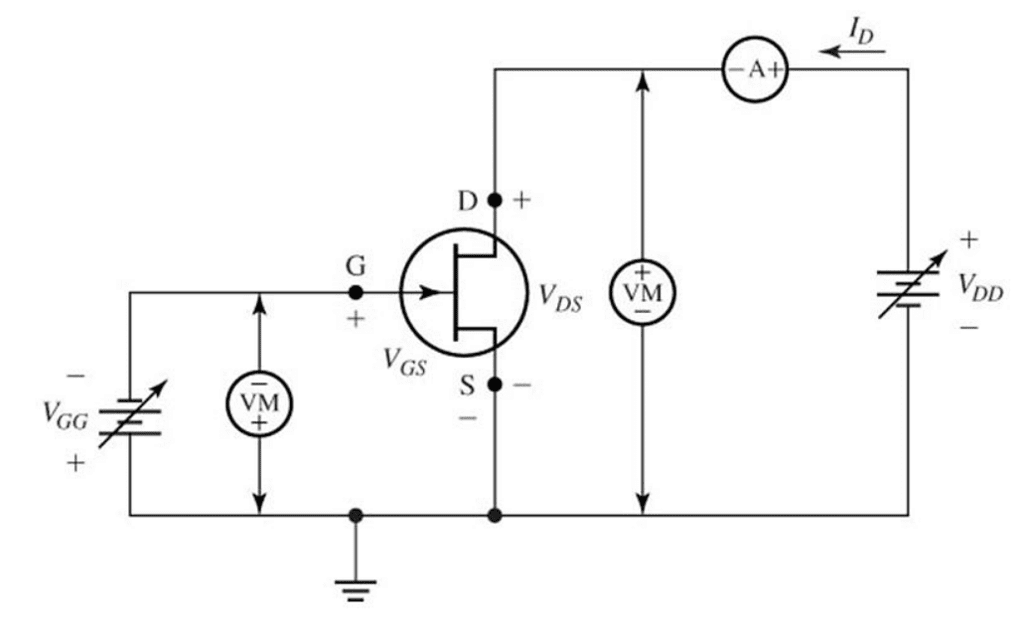 Experimental setup to plot JFET characteristics
- It is of course in principle not possible for the channel to close completely and thereby reduce the current Id to zero, if such indeed, could be the case the gate voltage Vgs is applied in the direction to provide additional reverse bias.
- When voltage is applied between the drain and source with a battery Vdd, the electrons flow from source to drain through the narrow channel existing between the depletion regions. This constitutes the drain current Id, its conventional direction is from drain to source.
- The value of drain current is maximum when no external voltage is applied between gate and source and is designated by Idss.
- When Vgs is increased beyond zero the depletion regions are widened. This reduces the effective width of the channel and therefore controls the flow of drain current through the channel.
- When Vgs is further increased a stage is reached at which to depletion regions touch each other that means the entire channel is closed with depletion region. This reduces the drain current to zero.
The document Field Effect Transistor | Analog and Digital Electronics - Electrical Engineering (EE) is a part of the Electrical Engineering (EE) Course Analog and Digital Electronics.
All you need of Electrical Engineering (EE) at this link: Electrical Engineering (EE)
|
135 videos|167 docs|71 tests
|
FAQs on Field Effect Transistor - Analog and Digital Electronics - Electrical Engineering (EE)
| 1. What is a Field Effect Transistor (FET) and how does it differ from other transistors? |  |
Ans. A Field Effect Transistor (FET) is a type of transistor that uses an electric field to control the flow of current. Unlike bipolar transistors, FETs have a high input impedance and do not require any current to control the output. This makes FETs ideal for applications where a small amount of input signal needs to control a larger output signal.
| 2. What are the different classifications of FETs? |  |
Ans. FETs can be classified into two main types: Junction Field Effect Transistors (JFETs) and Metal-Oxide-Semiconductor Field Effect Transistors (MOSFETs). JFETs are further classified as N-channel and P-channel based on the type of charge carriers they use. MOSFETs are classified as N-channel and P-channel as well, but they have an additional subcategory called Enhancement-mode and Depletion-mode MOSFETs.
| 3. How is an N-channel FET constructed and how does it operate? |  |
Ans. An N-channel FET is constructed using a piece of N-type semiconductor material between two P-type semiconductor regions. The middle N-type region is called the channel, and it is separated from the P-type regions by a thin insulating layer. When a positive voltage is applied to the gate terminal (Vgs), it creates an electric field that controls the flow of current through the channel. By varying the value of Vgs, the conductivity of the channel can be controlled, resulting in a varying output current.
| 4. How does varying the value of Vgs affect the operation of an N-channel FET? |  |
Ans. Varying the value of Vgs in an N-channel FET determines the level of the electric field applied to the gate terminal. Increasing Vgs beyond a certain threshold voltage turns on the FET, allowing current to flow through the channel. Decreasing Vgs below the threshold voltage turns off the FET, blocking the current flow. Therefore, by varying Vgs, the FET can be operated in different states, such as on or off.
| 5. What happens when both Vgs and Vds are applied to an N-channel FET? |  |
Ans. When both Vgs (gate-source voltage) and Vds (drain-source voltage) are applied to an N-channel FET, the FET operates in the saturation region. In this region, the FET is fully turned on, and the channel acts as a low resistance path for current flow. The output current is primarily determined by the value of Vgs, while Vds helps to maintain the FET in the saturation region.
Related Searches


