Biasing FET | Analog and Digital Electronics - Electrical Engineering (EE) PDF Download

BIASING FET:-
For the proper functioning of a linear FET amplifier, it is necessary to maintain the operating point Q stable in the central portion of the pinch off region. The Q point should be independent of device parameter variations and ambient temperature variations.
This can be achieved by suitably selecting the gate to source voltage Vgs and drain current Id which is referred to as biasing.
JFET biasing circuits are very similar to BJT biasing circuits. The main difference between JFET circuits and BJT circuits is the operation of the active components themselves.
There are mainly two types of Biasing circuits
- Self bias
- Voltage divider bias.
6.9.1 SELF BIAS
Self bias is a JFET biasing circuit that uses a source resistor to help reverse bias the JFET gate. A self bias circuit is shown in the fig. Self bias is the most common type of JFET bias. This JFET must be operated such that gate source junction is always reverse biased. This condition requires a negative Vgs for an N-channel JFET and a positive Vgs for P-channel JFET. This can be achieved using the self bias arrangement as shown in Fig. The gate resistor RG doesn’t affect the bias because it has essentially no voltage drop across it, and the gate remains at 0 V. RG is necessary only to isolate an ac signal from ground in amplifier applications. The voltage drop across resistor RS makes gate source junction reverse biased.
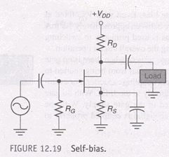
For the dc analysis, coupling capacitors are open circuits.
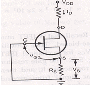
For the N channel FET in Fig (a)
IS produces a voltage drop across RS and makes the source positive w.r.t ground. In any JFET circuit all the source current passes through the device to the drain circuit. This is due to the fact that there is no significant gate current.
We can define source current as IS = ID
(VG =0 because there is no gate current flowing in RG. So, VG across RG is zero)
VG =0 then VS= ISRS =ID RS
VGS = VG-VS =0-ID RS=- ID RS
DC analysis of self Bias:-
In the following DC analysis, the N-channel JFET shown in the fig. is used for illustration.
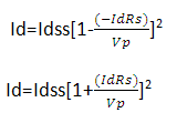
For DC analysis we can replace coupling capacitors by open circuits and we can also replace the resistor RG by a short circuit equivalent.:. IG = 0.The relation between ID and VGS is given by-
Id=Idss 

VGS for N-channel JFET is =-Id Rs
Substuting this value in the above equation,
For the N-chanel FET in the above figure
Is produces a voltage drop across Rs and makes the source positive w.r.t ground in any JFET circuit, all the source current passes through the device to drain circuit this is due to the fact that there is no significant gate current. Therefore, we can define source current as Is=Id and Vg=0 then
Vs= Is Rs =IdRs
Vgs=Vg-Vs=0-IdRs=-IdRs
Drawing the self bias line:-
Typical transfer characteristics for a self biased JFET are shown in the fig.
The maximum drain current is 6mA and the gate source cut off voltage is -3V. This means the gate voltage has to be between 0 and -3V.
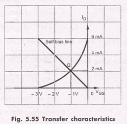
Now using the equation Vgs= -IDRS and assuming RS of any suitable value we can draw the self bias line.
Let us assume RS = 500Ω
With this Rs , we can plot two points corresponding to ID = 0 and ID = IDSS
for ID = 0
VGS = -ID RS
VGS = 0 x (500.Ω) = 0V
So the first point is (0 ,0)
( ID, VGS)
For ID= IDSS=6mA
VGS = (-6mA) (500 Ω) = -3V
So the 2nd Point will be (6mA,-3V)
By plotting these two points, we can draw the straight line through the points. This line will intersect the transconductance curve and it is known as self bias line.The intersection point gives the operating point of the self bias JFET for the circuit.
At Q point , the ID is slightly > than 2mA and VGS is slightly > -1V. The Q point for the self bias JFET depends on the value of RS. If RS is large, Q point is far down on the transconductance curve, ID is small, when RS is small Q point is far up on the curve , ID is large.
6.9.2 VOLTAGE DIVIDER BIAS:-
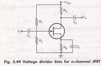
The fig. shows N channel JFET with voltage divider bias. The voltage at the source of JFET must be more positive than the voltage at the gate in order to keep the gate to source junction reverse biased. The source voltage is
VS = IDRS
The gate voltage is set by resistors R1 and R2 as expressed by the following equation using the voltage divider formula.
For dc analysis:
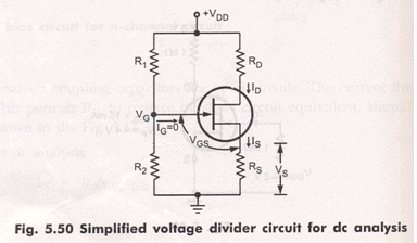
Applying KVL to the input circuit
VG-VGS-VS =0
:: VGS = VG-Vs=VG-ISRS
VGS = VG-IDRS :: IS = ID
Applying KVL to the input circuit we get
VDS+IDRD+VS-VDD =0
::VDS = VDD-IDRD-IDRS
VDS = VDD-ID ( RD +RS )
The Q point of a JFET amplifier , using the voltage divider bias is
IDQ = IDSS [1-VGS/VP]2
VDSQ = VDD-ID ( RD+RS )
COMPARISON OF MOSFET WITH JFET
- In enhancement and depletion types of MOSFET, the transverse electric field induced across an insulating layer deposited on the semiconductor material controls the conductivity of the channel.
- In the JFET, the transverse electric field across the reverse biased PN junction controls the conductivity of the channel.
- The gate leakage current in a MOSFET is of the order of 10-12A. Hence the input resistance of a MOSFET is very high in the order of 1010 to 1015 Ω. The gate leakage current of a JFET is of the order of 10-9A., and its input resistance is of the order of 108Ω.
- The output characteristics of the JFET are flatter than those of the MOSFET, and hence the drain resistance of a JFET (0.1 to 1MΩ) is much higher than that of a MOSFET (1 to 50kΩ).
- JFETs are operated only in the depletion mode. The depletion type MOSFET may be operated in both depletion and enhancement mode.
- Comparing to JFET, MOSFETs are easier to fabricate.
- Special digital CMOS circuits are available which involve near zero power dissipation and very low voltage and current requirements. This makes them suitable for portable systems.
|
135 videos|167 docs|71 tests
|
FAQs on Biasing FET - Analog and Digital Electronics - Electrical Engineering (EE)
| 1. What is FET biasing in electrical engineering? |  |
| 2. Why is biasing important in FET circuits? | |
| 3. What are the different methods of biasing a FET? | |
| 4. How does FET biasing affect the amplifier's gain? | |
| 5. What are the advantages and disadvantages of different FET biasing methods? | |


MCQs
,video lectures
,Summary
,study material
,Objective type Questions
,Semester Notes
,Exam
,past year papers
,Sample Paper
,Free
,Biasing FET | Analog and Digital Electronics - Electrical Engineering (EE)
,Viva Questions
,mock tests for examination
,Biasing FET | Analog and Digital Electronics - Electrical Engineering (EE)
,shortcuts and tricks
,practice quizzes
,Biasing FET | Analog and Digital Electronics - Electrical Engineering (EE)
,Extra Questions
,Previous Year Questions with Solutions
,Important questions
,ppt
;


Biasing FET Free PDF Download
Importance of Biasing FET
Biasing FET Notes
Biasing FET Electrical Engineering (EE) Questions
Study Biasing FET on the App
|
© EduRev
|
Education Revolution
|


|


