BCD to 7 Segment | Analog and Digital Electronics - Electrical Engineering (EE) PDF Download
BCD-to-Decimal Decoder
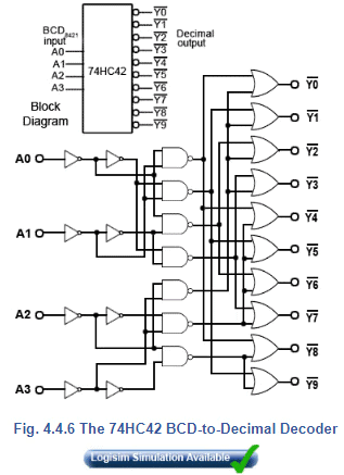
The 74HC42 BCD-to-Decimal decoder IC from Texas Instruments contains a more complex circuit, as illustrated in both block and logic schematic form in Fig. 4.4.6.
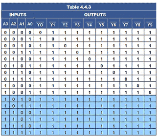
The input is in 4-bit BCD8421 format, and each of the ten outputs, labelled produce a logic 0 for an appropriate BCD8421 input of 00008421 to 01018421. Any input value greater than 01018421 results in all of the output pins remaining at their high level, as shown in pale blue in Table 4.4.3.
Note that the truth table (Table 4.4.3) shows the appropriate high and low logic levels as 1 and 0 respectively to match the logic levels shown in the downloadable Logisim simulation.
On most data sheets for ICs the levels are shown as H (the higher voltage) and L (the lower voltage) to avoid confusion in cases where negative logic is used.
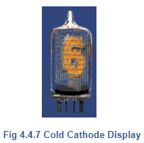
BCD to decimal decoders were originally used for driving cold cathode numerical displays (Nixie tubes), which are neon filled glass plug-in tubes with ten anodes in the shape of numbers 0 to 9 that glow when activated by a high voltage.
However, decimal decoders are also useful for a variety of other uses. Remember that decoders are often also called demultiplexers, as they can be used for many demultiplexing tasks and for driving devices such as lamps, motors and relays in control systems.
BCD to 7 Segment Decoders
Because cold cathode displays require a high voltage drive, they have mostly been replaced by low voltage LED or LCD displays using 7 segment displays, therefore the BCD-to-7-segment decoder has become one of the most commonly available decoders.
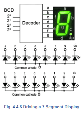
As shown in block diagram format in Fig. 4.4.8, this type of decoder has 4 inputs for binary coded decimal and an output for each of the 7 LEDs that make up the 7-segment display. The eighth LED (labelled dp or sometimes h) will normally be controlled by some extra logic outside the decoder. 7-segment displays may have a common cathode connection, needing to be driven by logic 1 outputs, or common anode connection requiring logic 0 outputs from the decoder.
Decoder/Drivers
Depending on the decoder IC and display type used, although it may sometimes be necessary to use a transitor amplifier to drive each segment of the display, there are Decoder/Driver ICs available, such as the 74LS46, 47, 48 and 49 that have sufficient output current and a choice of output designs such as open collector, internal pullup resistors and active high or active low output levels that allow direct connection to both led and filament lamp displays.
7-Segment Fonts
When illuminated by the correct logic levels, the seven-segment display will show all the decimal numbers from 0 to 9. Depending on the logic design of the IC, some decoders will automatically blank the display for any value greater than 9, while others display a unique (non-numeric) pattern for each value from 10 to 15 as shown in Fig. 4.4.9, and may display 6 and 9 with or without a ‘tail’. For displaying Hexadecimal numbers, the letters A b C d E and F are used to avoid confusion between capital B and 8, and capital D and 0.

4LS49 BCD to 7-Segment Decoder
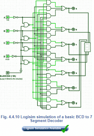
Fig. 4.4.10 is a screen grab from Logisim, showing a working simulation of a basic BCD to 7-segment decoder (based on the 74LS49 in the TTL range of 7-segment decoders from Texas Instruments. This IC uses the font illustrated in Fig. 4.4.9 and a single active low BI pin for use as a blanking input.
Blanking
The blanking input pin BI can be used to turn off the display to reduce power consumption, or it can be driven with a variable width pulse waveform to rapidly switch the display on and off thereby varying the apparent brightness of the display.
Making the BI input logic 0 blanks the display whatever data is present at the decoder BCD inputs.
74LS48 BCD to 7-Segment Decoder Features
Ripple Blanking
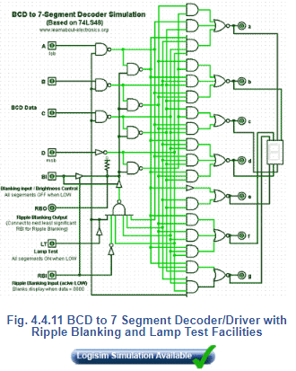
As a BCD to 7 Segment decoder is designed to drive a single 7 segment display, each digit of a numeric display is driven by a separate decoder, so where multiple digits are required, a technique called Ripple Blanking is used, this allows the blanking inputs of several ICs to be connected in cascade. The Ripple Blanking Output (RBO) of the first decoder IC (controlling the most significant digit) is fed to the blanking input pin of the next most significant digit decoder and so on.
When Logic 0 is applied to the ripple blanking input (RBI) of a decoder, it blanks the display only when the BCD input to that particular decoder is 0000. A logic 0 input will therefore blank any display digit that is 0. This allows for the suppression of any leading or trailing zeros in numbers such as 00000077 or 7.7000000.
There are a number of BCD-to-7-segment decoder ICs in the 74 series (types 7446 to 7449) each with different variations, such as active high or active low outputs, high current driver outputs, a choice of display font (whether the 6 and the 9 have a ‘tail’ or not), and a lamp test input to check that all LEDs are working.
Fig. 4.4.11 is a screen grab of a BCD to 7-segment decoder using these advanced features. Click the ‘Simulation Available’ button to download a working simulation for this circuit. Note that although the simulation works in a similar manner to a real decoder such as the 74LS48, because the BI input and RBO output on the real chip share a common pin, this creates problems for the simulator. Therefore the logic has been changed by using two tri-state buffers to separate the input and output signals.
Tri-State Logic
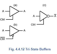
The simulation illustrated in Fig. 4.4.11 uses two tri-state buffers(also called 3-state buffers) to achieve isolation between a shared input and output pin. The necessary isolation was achieved by using two simple tri-state buffers, shown in Fig 4.4.12 so that the shared pin can be an input or an output, but not at the same time.
The tri-state buffer (a) in Fig. 4.4.12 has an input and an output just like a normal buffer, but it also has a control (Ctrl) input. This input, when held at logic 1 enables the buffer, so whatever logic level appears at its input also appears at its output.
When logic 0 is applied to the Ctrl input however, the buffer is disabled and its output assumes a high impedance state. That is, it will take up whatever logic level occurs on the line connected to its output, no matter what logic level is on its input. It is effectively open circuit, just as though making the enable input low had opened a switch between its input and output.
Tri-state buffers are also available with an active low Ctrl input, that are enabled by logic 0 (b), and as inverting buffers, that invert the output when Ctrl is activated (c).
There are whole ranges of devices that have 3-state outputs. Devices such as microprocessors and memory chips, intended for use in bus systems, where many inputs and outputs share a common connection (e.g. a data bus) normally have tri-state outputs. However, apart from very large scale integrated (VLSI) devices, such as computer ICs, 3-state logic is not generally used within MSI ICs as shown in Fig 4.4.11. In these smaller scale ICs, alternatives such as open collector logic are more suitable. Discrete 3-state logic components are more often used for connections between, rather than within ICs
Latching BCD-to-7-Segment Decoders
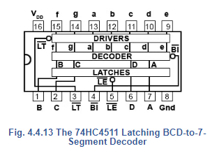
In common with modern practice, TTL ICs are not generally recommended for new designs and are superseded by newer HC and HCT versions. Apart from the advantage of lower power on these versions, a common feature added to these ICs is a ‘Data Latch’. This is a one nibble memory (for the 4 bit BCD input) controlled by a Latch Enable (LE) pin, which allows the decoder to store the 4 bit input present, when LE is logic 0 so that only the stored data is displayed. When the latch is not enabled however, it becomes ‘transparent’ i.e. any changes in the data appearing at the inputs are fed directly to the display. It is also common on later ranges of decoders that any input values greater than 1001BCD (910) are automatically blanked. Fig. 4.4.13 shows a typical pin-out for a CMOS BCD-to-7-segment decoder. Examples of these ICs are the MC14513 from ON Semiconductors and the 74HC4511 from NXP Philips Semiconductors.
 |
Download the notes
BCD to 7 Segment
|
Download as PDF |
Address Decoders
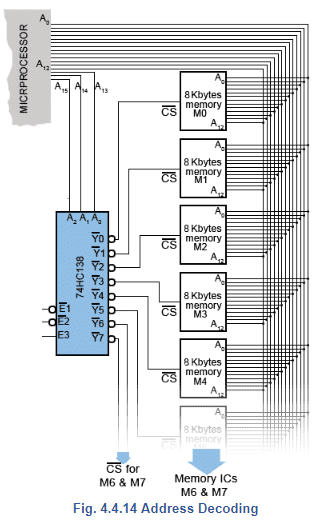
Decoders may also be used in computer systems for address decoding. Fig. 4.4.14 illustrates a typical application where a 74HC1387 3-to-8-line decoder is used to enable the microprocessor to communicate with many locations in its memory system. The memory in this example comprises 8 x 8 Kbyte memory ICs, therefore each IC contains 8192 x 1 byte locations giving a total number of 8 x 8192 = 65536 locations, each having a hexadecimal location number (an address) from 000016 to FFFF16.
To contact any of these memory locations, the microprocessor outputs the address of the required memory location on the 16-bit address bus, which can hold any one of 216 = 65536 different values. However, the memory in this example is made up from 8 identical ICs, each holding 8192 locations, and as this number of locations can be addressed by 213 = 13 address lines, lines (A0 to A12) are connected from the microprocessor to the 13 address inputs of each memory IC. This common connection means that each of the memory chips will have the same address range as all the other memory ICs, and therefore any address within the range 000016 to 200016 (819210) put out by the microprocessor will contact the same address in all 8 memory ICs. This obviously creates a problem; each memory chip should have its own range of addresses with the 8 ICs forming a continuous address sequence in blocks of 819210 locations.
This is where the address decoder is used. Notice that, in Fig. 4.4.14 the three highest order address lines (A13, A14 and A15) are connected to the 3 address inputs (A0, A1 and A2) of the 74HC138 3-to-8-line decoder. Therefore, provided that the three Enable inputs of the decoder are fed with the appropriate logic levels to enable the decoder, each of the
pins of the decoder will output a logic 0 for one of the 8 possible combinations of the three bit value on the address lines A13 to A15.Since this three bit value will only change when the 16-bit value on the address bus changes by 819210 (200016) the memory chips will be selected using their chip select
inputs, every 8 Kbytes. The eight memory ICs will therefore provide a sequential set of memory locations covering the whole 64K of memory, addressable by the microprocessor.
The 74HC138 Decoder
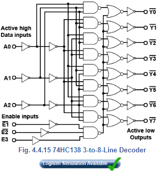
The combinational logic of a typical 3-to-8-line decoder based on the 74HC138, is illustrated in Fig. 4.4.15, an IC that has many uses apart from address decoding, it is often used with a binary counter driving its inputs, when its eight outputs constantly step through a 0 to 7 sequence. Typical applications include sequence generating for lamp control, row scanning for dot matrix displays, digital operation of analogue controls and anywhere that a sequence of unique outputs is required.
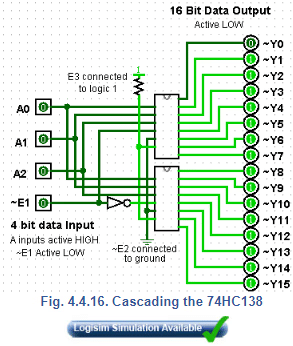
Data sheets for the 74HC138 point out the advantages of the three Enable pins, which can be used for simply connecting the decoders together to make larger decoders. An example of this is shown in the downloadable Logisim simulation Fig. 4.4.16, where two 74HC138 ICs are connected together using only one additional NOT gate.
Note that the pin connections on the ICs in Fig. 4.4.16 are not in the consecutive 1 to 16 order of the real 74HC138 pinout, but can be identified in the downloaded simulation by hovering your mouse over any pin.
The (active LOW) input is used here as the fourth (23) data input so that for a count of 0 to 710 (00002 to 01112) at the inputs, the logic 0 applied to
enables the top IC and disables the bottom IC via the NOT gate, but for a count between 10002 and 11112 )810 to 1510)the fourth data input
becomes logic 1 and the situation is reversed, with the (active low) output continuing its (810 to 1510) sequence on the bottom IC.
Conclusion
The study of BCD-to-Decimal and BCD-to-7-segment decoders, along with their advanced features like blanking, ripple blanking, and address decoding (e.g., 74HC138), highlights their importance in digital electronics for GATE ECE. These circuits, from the 74HC42 to the 74HC4511, offer practical solutions for displays and memory systems, encouraging learners—reminded by “Don’t fear failure. Fear being in the exact same place next year as you are today”—to master them for exam success and innovation.
|
137 videos|144 docs|71 tests
|
FAQs on BCD to 7 Segment - Analog and Digital Electronics - Electrical Engineering (EE)
| 1. What is a BCD code and how is it used in 7-segment displays? |  |
| 2. How does the BCD to 7-segment decoder circuit work? |  |
| 3. Can the BCD to 7-segment decoder circuit display numbers greater than 9? |  |
| 4. Are there any limitations or drawbacks of using a BCD to 7-segment decoder circuit? |  |
| 5. What are some common applications of BCD to 7-segment decoder circuits? |  |


