D-Type Flip-Flops and Toggle Flip-Flops | Digital Electronics - Electrical Engineering (EE) PDF Download

D Type Flip-flops
The major drawback of the SR flip-flop (i.e. its indeterminate output and non-allowed logic states) described in Digital Electronics Module 5.2 is overcome by the D type flip-flop. This flip-flop, shown in Fig. 5.3.1 together with its truth table and a typical schematic circuit symbol, may be called a Data flip-flop because of its ability to ‘latch’ and remember data, or a Delay flip-flop because latching and remembering data can be used to create a delay in the progress of that data through a circuit. To avoid the ambiguity in the title therefore, it is usually known simply as the D Type.
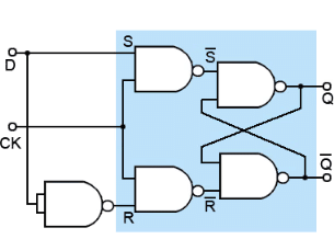
The simplest form of D Type flip-flop is basically a high activated SR type with an additional inverter to ensure that the S and R inputs cannot both be high or both low at the same time. This simple modification prevents both the indeterminate and non-allowed states of the SR flip-flop. The S and R inputs are now replaced by a single D input, and all D type flip-flops have a clock input.
Operation
As long as the clock input is low, changes at the D input make no difference to the outputs. The truth table in Fig. 5.3.1 shows this as a ‘don’t care’ state (X). The basic D Type flip-flop shown in Fig. 5.3.1 is called a level triggered D Type flip-flop because whether the D input is active or not depends on the logic level of the clock input.
Provided that the CK input is high (at logic 1), then whichever logic state is at D will appear at output Q and (unlike the SR flip-flops)  is always the inverse of Q).
In Fig. 5.3.1, if D = 1, then S must be 1 and R must be 0, therefore Q is SET to 1.
Alternatively,
If D = 0 then R must be 1 and S must be 0, causing Q to be reset to 0.
The Data Latch
The name Data Latch refers to a D Type flip-flop that is level triggered, as the data (1 or 0) appearing at D can be held or ‘latched’ at any time whilst the CK input is at a high level (logic 1).
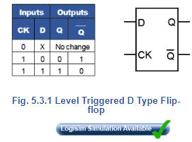
As can be seen from the timing diagram shown in Fig 5.3.2, if the data at D changes during this time, the Q output assumes the same logic level as the D.
Ripple Through
Fig. 5.3.2 also illustrates a possible problem with the level triggered D type flip-flop; if there are changes in the data during period when the clock pulse is at its high level, the logic state at Q changes in sympathy with D, and only ‘remembers’ the last input state that occurred during the clock pulse, (period RT in Fig. 5.3.2). This effect is called ‘Ripple Through’, and although this allows the level triggered D Type flip-flop to be used as a data switch, only allowing data through from D to Q as long as CK is held at logic 1, this may not be a desirable property in many types of circuit.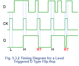
The Edge Triggered D Type Flip-flop
Fortunately ripple though can be largely prevented by using the Edge Triggered D Type flip-flop illustrated in Fig 5.3.3.
The clock pulse applied to the flip-flop is reduced to a very narrow positive going clock pulse of only about 45ns duration, by using an AND gate and applying the clock pulse directly to input ‘a’ but delaying its arrival at input ‘b’ by passing it through 3 inverters. This inverts the pulse and also delays it by three propagation delays, (about 15ns per inverter gate for 74HC series gates). The AND gate therefore produces logic 1 at its output only for the 45ns when both ‘a’ and ‘b’ are at logic 1 after the rising edge of the clock pulse.
Synchronous and Asynchronous Inputs
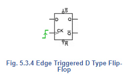
A further refinement in Fig. 5.3.3 is the addition of two further inputs SET and RESET, which are actually the original S and Rinputs of the basic low activated SR flip-flop.
Notice that there is now a subtle difference between the active low Set  and Reset
  inputs, and the D input. The D input is SYNCHRONOUS, that is its action is synchronised with the clock, but the
  inputs are ASYNCHRONOUS i.e. their action is NOT synchronised with the clock. The SET and RESET inputs in Fig 5.3.4 are ‘low activated’, which is shown by the inversion circles at the S and R inputs to indicate that they are really .
The flip-flop is positive edge triggered, which is shown on the CK input in Fig 5.3.4 by the wedge symbol. A wedge accompanied by an inversion circle would indicate negative (falling) edge triggering, though this is generally not used on D Type flip-flops.
Timing Diagram
The ‘Edge triggered D type flip-flop with asynchronous preset and clear capability’, although developed from the basic SR flip-flop becomes a very versatile flip-flop with many uses. A timing diagram illustrating the action of a positive edge triggered device is shown in Fig. 5.3.5.
At the positive going edges of clock pulses a and b, the D input is high so Q is also high.
Just before pulse c the D input goes low, so at the positive going edge of pulse c, Q goes low.
Between pulses c and d the asynchronous  input goes low and immediately sets Q high.
The flip-flop then ignores pulse d while is low, but as returns high, and D has also returned to its high state before pulse e, Q remains high during pulse e.
At the positive going edge of pulse h, the low level of input D remains, keeping Q low, but between pulses h and i, the S input goes low, overriding any action of D and immediately making Q high.
D is still high at the positive going edge of pulse f, and because the flip-flop is positive edge triggered, the change in the logic level of D during pulse f is ignored until the positive going edge of pulse g, which resets Q to its low level.
Clock pulse i is again ignored, due to being in its active low state and Q remains high, under the control of until just before pulse j. At the positive going edge of pulse j, input D regains control, but as D is high and Q is already high, no change in output Q occurs.
Finally, just before pulse k, the asynchronous reset input  goes low and resets Q to its low level (logic 0), which again causes the D input to be ignored.
The Toggle Flip-flop
Toggle flip-flops are the basic components of digital counters, and all of the D type devices are adaptable for such use. When an electronic counter is used for counting, what are actually being counted are pulses appearing at the CK input, which may be either regular pulses derived from an internal clock, or they can be irregular pulses generated by some external event.
When a toggle flip-flop is used as one stage of a counter, its Q output changes to the opposite state, (it toggles) high or low on each clock pulse. Most edge-triggered flip-flops can be used as toggle flip-flops including the D type, which can be converted to a toggle flip-flop with a simple modification. In theory all that is necessary to convert an edge triggered D Type to a T type is to connect the Q output directly to the D input as shown in Fig. 5.3.8. The actual input is now CK. The effect of this mode of operation is also shown in the timing diagram in Fig. 5.3.8 using a positive edge triggered D type flip-flop.
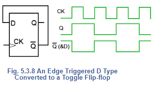
Toggle Flip-flop Operation
Suppose that initially CK and Q = 0. Then  and D must be 1. At the rising edge of a CK pulse, the logic 1 at D is allowed into the flip-flop and, at the end of the flip-flop’s propagation delay, appears at Q, and changes to logic 0 at the same time.
This logic 0 is now fed back to D, but it is important that it is not immediately accepted into the D input, otherwise oscillation could occur with D continually changing between 1 and 0. However, because of the flip-flop’s propagation delay, when the logic 0 from arrives at D, the very short edge-triggering period will have completed, and the change in data at D will be ignored.
At the next CK rising edge of the clock signal, the 0 at D now passes to Q, making and D logic 1 again. The Q output of the flip-flop therefore toggles at each positive going edge of the CK pulse.
Because the Q output changes state at each clock pulse rising edge, the 0 period and the 1 period of the Q output will always be of equal length, and the output will be a square wave with a 1:1 mark to space ratio, its frequency will be half that of CK.
To use toggle flip-flops as simple binary counters, a number of toggle flip-flops may be connected in cascade, with the Q output of the first flip-flop in the series, being connected to the CK input of the next flip-flop and so on. This is also the principle of frequency division. Exactly how counters and dividers can be constructed from toggle flip-flops is explained in Sequential Logic Module 5.6
Data Timing
In practice however, using direct feedback from to D can cause problems as, to ensure stable operation and avoid unwanted oscillation, it is important in any digital circuit, that any changes in logic level taking place at D must be both stable, (free from any overshoot or ringing etc.) and at a valid logic level during a short period, before and after the clock signal causes a change. These periods are called the set up and hold times.
Although it is easy to think of the clock signal initiating a change at a particular time, e.g. when its rising edge occurs, data is actually clocked into input D when the CK waveform reaches a certain voltage level. In 74HC series gates this level is 50% of VDD, as illustrated in Fig 5.3.9. This shows in expanded time detail, the transitions taking place at the D and CK inputs of a D type positive edge triggered flip-flop.
To guarantee correct triggering, it is important that the data at the D input has settled at a valid logic level before the clock signal triggers any change. Therefore there must be some time allowed from when the D input first becomes valid to allow time for any slow rising pulse, any overshoot or ringing to occur before the clock pulse samples the logic level.
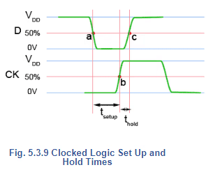 For example, the time between point (a) in Fig.5.3.9, where D initially falls below 50% of VDD and the time when CK rises to its trigger threshold of 50% VDD (point b) is called the set up time (tsetup or tsu), and in 74HC series ICs this will typically be between 5ns and 15ns.
After the trigger point there must be a further period (b to c in Fig. 5.3.9) where the data at D must remain at the same valid logic level to ensure that the correct logic level has been accepted. This is called the hold time (thold or th) and is typically around 3ns in 74HC series ICs.
In sequential logic circuits, precise timing is vitally important. The design of a circuit must take into consideration not only set up and hold times but also the propagation times of gates or flip-flops in each path that a digital signal takes through a circuit. Failure to get the timing right can lead to problems such as ‘glitches’ i.e. sudden sharp spikes, as a device such as a flip-flop momentarily produces a change from one logic level to another and back again. Such glitches may be very short (a few nanoseconds) but sufficient to trigger another device to a wrong logic level.
With devices such as flip-flops using both triggering and feedback, incorrect timing can also lead to instability and unwanted oscillations. Avoiding such problems is a major reason for the use of edge triggering and master slave devices.
D Type Flip-flop ICs
A selection of D type Flip-flop ICs are listed below.
- 74CH74 Dual D Type Flip-flop with Set and Reset from ON Semiconductors.
- 74LS75 Quad D Type Data Latches from Texas instruments.
- 74CH174 Hex D Type Flip-flop with Reset from NXP.
- 74CH175 Quad D Type Flip-flop with Reset from NXP.
- 74CH273 Octal D Type Flip-flop with Reset from Texas instruments.
- 74CH373 Octal Transparent D Type Data Latches with 3-State Outputs from Texas instruments.
- 74CH374A Octal 3-State Non-Inverting D Type Flip-flop from ON Semiconductors.
|
125 videos|83 docs|58 tests
|
FAQs on D-Type Flip-Flops and Toggle Flip-Flops - Digital Electronics - Electrical Engineering (EE)
| 1. What is a D-Type Flip Flop? |  |
| 2. How does a D-Type Flip Flop differ from an S-R Flip Flop? | |
| 3. What is the advantage of using D-Type Flip Flops? | |
| 4. How do S-R Flip Flops work? | |
| 5. Can a D-Type Flip Flop be used as an S-R Flip Flop? | |


Extra Questions
,Free
,Summary
,Sample Paper
,video lectures
,D-Type Flip-Flops and Toggle Flip-Flops | Digital Electronics - Electrical Engineering (EE)
,Semester Notes
,shortcuts and tricks
,D-Type Flip-Flops and Toggle Flip-Flops | Digital Electronics - Electrical Engineering (EE)
,past year papers
,Previous Year Questions with Solutions
,ppt
,study material
,Exam
,mock tests for examination
,Objective type Questions
,MCQs
,Important questions
,practice quizzes
,D-Type Flip-Flops and Toggle Flip-Flops | Digital Electronics - Electrical Engineering (EE)
,Viva Questions
;


D-Type Flip-Flops and Toggle Flip-Flops Free PDF Download
Importance of D-Type Flip-Flops and Toggle Flip-Flops
D-Type Flip-Flops and Toggle Flip-Flops Notes
D-Type Flip-Flops and Toggle Flip-Flops Electrical Engineering (EE) Questions
Study D-Type Flip-Flops and Toggle Flip-Flops on the App
|
© EduRev
|
Education Revolution
|


|


