


All Exams >
NEET >
1 Year Dropper Course for NEET >
All Questions
All questions of Semiconductor Electronics: Materials, Devices & Simple Circuits for NEET Exam
Arrange the materials in ascending order of energy band gaps- a)conductor, semiconductor, insulator
- b)insulator, semiconductor, conductor
- c)semiconductor, conductor, insulator
- d)insulator, conductor, semiconductor
Correct answer is option 'A'. Can you explain this answer?
Arrange the materials in ascending order of energy band gaps
a)
conductor, semiconductor, insulator
b)
insulator, semiconductor, conductor
c)
semiconductor, conductor, insulator
d)
insulator, conductor, semiconductor
|
|
Krishna Iyer answered |
- In the case of insulators, the energy gap is very large while in the case of conductors energy gap is very short.
- This energy gap refers to the energy difference between the valence band and conduction band whereas, in semiconductors, this band gap value is in between that of conductors and insulators.

Can you explain the answer of this question below:When a pure semiconductor is heated, its resistance- A:Goes down.
- B:Goes up.
- C:Remains the same.
- D:None of the above.
The answer is a.
When a pure semiconductor is heated, its resistance
A:
Goes down.
B:
Goes up.
C:
Remains the same.
D:
None of the above.
|
|
Nikita Singh answered |
As temperature increases electrons from the valence band go to the conduction band, so conductivity increases hence resistance decreases.
The densities of electrons and holes in an extrinsic semiconductor are 8 x 1015 cm-3and 5 x 1012 cm-3 respectively. The mobilities of electrons and holes are respectively 23 x 103 cm3 / Vs and 102 cm3 / Vs. Which type of semiconductor is it?- a)p-type only
- b)n-type only
- c)either n or p type
- d)both n and p type
Correct answer is option 'B'. Can you explain this answer?
The densities of electrons and holes in an extrinsic semiconductor are 8 x 1015 cm-3and 5 x 1012 cm-3 respectively. The mobilities of electrons and holes are respectively 23 x 103 cm3 / Vs and 102 cm3 / Vs. Which type of semiconductor is it?
a)
p-type only
b)
n-type only
c)
either n or p type
d)
both n and p type
|
|
Maulik Dasgupta answered |
Given data:
- Density of electrons (n) = 8 x 10^15 cm^-3
- Density of holes (p) = 5 x 10^12 cm^-3
- Mobility of electrons (μn) = 23 x 10^3 cm^2/ V s
- Mobility of holes (μp) = 10^2 cm^2/ V s
To determine the type of semiconductor, we need to compare the densities of electrons and holes.
Explanation:
- In an n-type semiconductor, the majority charge carriers are electrons, and the minority charge carriers are holes. The density of electrons is much higher than the density of holes.
- In a p-type semiconductor, the majority charge carriers are holes, and the minority charge carriers are electrons. The density of holes is much higher than the density of electrons.
Now we can compare the given densities of electrons and holes:
- Density of electrons (n) = 8 x 10^15 cm^-3 (very high)
- Density of holes (p) = 5 x 10^12 cm^-3 (very low)
This indicates that the majority charge carriers are electrons, and the semiconductor is n-type.
We can also check the mobility values to confirm this:
- Mobility of electrons (μn) = 23 x 10^3 cm^2/ V s (very high)
- Mobility of holes (μp) = 10^2 cm^2/ V s (very low)
The high mobility of electrons also supports the conclusion that the semiconductor is n-type.
Therefore, the correct answer is option (B) n-type only.
Can you explain the answer of this question below:What is the order of forbidden gap in the energy bands of silicon?
- A:
3.1 eV
- B:
0.1 eV
- C:
2.1 eV
- D:
1.1 eV
The answer is d.
What is the order of forbidden gap in the energy bands of silicon?
3.1 eV
0.1 eV
2.1 eV
1.1 eV
|
|
Anjali Iyer answered |
Eg : Silicon & Germanium. b) For silicon forbidden energy gap is 1.1 eV and for germanium 0.72 eV. c) At absolute zero, semiconductors behave as perfect insulators. d) Semiconductors are of two types.
A semiconductor is formed by- a)Covalent bonds
- b)Electrovalent bonds
- c)Coordinate bonds
- d)None of above
Correct answer is option 'A'. Can you explain this answer?
A semiconductor is formed by
a)
Covalent bonds
b)
Electrovalent bonds
c)
Coordinate bonds
d)
None of above
|
|
Wahid Khan answered |
The electrons surrounding each atom in a semiconductor are part of a covalent bond. A covalent bond consists of two atoms "sharing" a single electron. Each atom forms 4 covalent bonds with the 4 surrounding atoms. Therefore, between each atom and its 4 surrounding atoms, 8 electrons are being shared.##
The binary number 10101 is equivalent to decimal number- a)21
- b)13
- c)43
- d)51
Correct answer is option 'A'. Can you explain this answer?
The binary number 10101 is equivalent to decimal number
a)
21
b)
13
c)
43
d)
51
|
|
Mira Joshi answered |
10101 is the binary number to be converted to a decimal number.
To convert, multiply the numbers individually with 2n where n changes according to place value of the number.
(10101)2= (20× 1) + (0 × 21) + (1×22) + (0×23) + (1×24)
= 1 + 0 + 4 + 0 + 16
= 21
To convert, multiply the numbers individually with 2n where n changes according to place value of the number.
(10101)2= (20× 1) + (0 × 21) + (1×22) + (0×23) + (1×24)
= 1 + 0 + 4 + 0 + 16
= 21
Can you explain the answer of this question below:If A = 1 and B = 0, what is the value of A.A+B?
A: AB: A2 + BC: A.BD: BThe answer is a.
A: A
B: A2 + B
C: A.B
D: B
The answer is a.

|
Ambition Institute answered |
A=1 and B=0
A.A+B
=A2+B [De-Morgan’s theorem)
=1+0
=1
=A
A.A+B
=A2+B [De-Morgan’s theorem)
=1+0
=1
=A
In a semiconductor, the energy gap between valence band and conduction band is abouta)10 eVb)5 eVc)1 eVd)15 eVCorrect answer is option 'C'. Can you explain this answer?
|
|
Riya Banerjee answered |
In semiconductors, the forbidden gap between the valence band and conduction band is very small. It has a forbidden gap of about 1 electron volt (eV).
Mobilities of electrons and holes in a sample of intrinsic germanium semiconductor at room temperature are 0.36m2/volt-sec and 0.17 m2/volt-sec respectively. If the electron and hole densities are each equal to 2.5 X 10¹⁹/m3, the conductivity is ______.
- a)1.22 S/m
- b)3.12 S/m
- c)4.12 S/m
- d)2.12 S/m
Correct answer is option 'D'. Can you explain this answer?
Mobilities of electrons and holes in a sample of intrinsic germanium semiconductor at room temperature are 0.36m2/volt-sec and 0.17 m2/volt-sec respectively. If the electron and hole densities are each equal to 2.5 X 10¹⁹/m3, the conductivity is ______.
a)
1.22 S/m
b)
3.12 S/m
c)
4.12 S/m
d)
2.12 S/m
|
|
Krishna Iyer answered |
Given in question,
Mobilities of electrons μe = 0.36×m2V−1s−1
Mobilities of holes μh = 0.17×m2V−1s−1
densities of electron= densities of holes=2.5×10¹⁹m−3
As we know, conductivity,
σ=1/p=e(μene+μnnn)
=1.6×10⁻¹⁹[0.36×2.5×1019+0.17×2.5×1019)]
=2.12Sm−1
σ=1/p=e(μene+μnnn)
=1.6×10⁻¹⁹[0.36×2.5×1019+0.17×2.5×1019)]
=2.12Sm−1
So the electrical conductivity of germanium is 2.12Sm−1
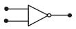
Can you explain the answer of this question below:The inputs of a NAND gate are connected together. The resultant circuit is
- A:
NOT gate
- B:
AND gate
- C:
OR gate
- D:
None of the above
The answer is a.
The inputs of a NAND gate are connected together. The resultant circuit is
NOT gate
AND gate
OR gate
None of the above
|
|
Lavanya Menon answered |
The equation of NAND gate is
Y=Aˉ.Bˉ
When both the terminals are connected together.
A=B=A
Y=Aˉ.Aˉ=Aˉ.Aˉ=Aˉ
Which is nothing but the equation of NOT gate.
Y=Aˉ
Option A is the correct answer.
Y=Aˉ.Bˉ
When both the terminals are connected together.
A=B=A
Y=Aˉ.Aˉ=Aˉ.Aˉ=Aˉ
Which is nothing but the equation of NOT gate.
Y=Aˉ
Option A is the correct answer.
The NOR gate is OR gate followed by- a)AND gate
- b)OR gate
- c)NOT gate
- d)None of the above
Correct answer is option 'C'. Can you explain this answer?
The NOR gate is OR gate followed by
a)
AND gate
b)
OR gate
c)
NOT gate
d)
None of the above
|
|
Rohit Shah answered |
A NOR gate is a logic gate which gives a positive output only when both inputs are negative. Like NAND gates, NOR gates are so-called "universal gates" that can be combined to form any other kind of logic gate.
The binary number system has a base of- a)8
- b)2
- c)10
- d)16
Correct answer is 'B'. Can you explain this answer?
The binary number system has a base of
a)
8
b)
2
c)
10
d)
16
|
|
Tanvi Bose answered |
Explanation:
Therefore, the correct answer to the question is option B, which states that the binary number system has a base of 2.
- The binary number system is a positional number system with a base of 2.
- It uses only two digits - 0 and 1 - to represent all numbers and values.
- Each digit in a binary number represents a power of 2, with the rightmost digit representing 2^0 (1), the next digit representing 2^1 (2), the next digit representing 2^2 (4), and so on.
- Binary numbers are used extensively in computer science and digital electronics because they can be easily represented using electronic circuits, and because the two digits can be easily translated into the on/off states of electronic switches.
Therefore, the correct answer to the question is option B, which states that the binary number system has a base of 2.
The name of a diode that can be used to provide a variable capacitance is:- a)varactor diode
- b)varactor capacitor
- c)potential diode
- d)potential capacitor
Correct answer is option 'A'. Can you explain this answer?
The name of a diode that can be used to provide a variable capacitance is:
a)
varactor diode
b)
varactor capacitor
c)
potential diode
d)
potential capacitor

|
Dr Manju Sen answered |
The varactor diode is used in a place where the variable capacitance is required, and that capacitance is controlled with the help of the voltage. The Varactor diode is also known as the Varicap, Voltcap, Voltage variable capacitance or Tunning diode.


What is the value of dielectric constant of a air ?- a) Less than 1
- b)Zero
- c)Equal to 1
- d) Not determine
Correct answer is option 'C'. Can you explain this answer?
What is the value of dielectric constant of a air ?
a)
Less than 1
b)
Zero
c)
Equal to 1
d)
Not determine
|
|
Ambition Institute answered |
The dielectric constant of a medium K = ∈/∈0
where ∈ is the permittivity of the medium.
For air, ∈ = ∈0
⟹ K = 1
where ∈ is the permittivity of the medium.
For air, ∈ = ∈0
⟹ K = 1
The device that can act as a complete electroniccircuit is [2010]- a)junction diode
- b)integrated circuit
- c)junction transistor
- d)zener diode
Correct answer is option 'B'. Can you explain this answer?
The device that can act as a complete electroniccircuit is [2010]
a)
junction diode
b)
integrated circuit
c)
junction transistor
d)
zener diode

|
Rajeev Sharma answered |
Integrated circuit can act as a complete
electronic circuit.
electronic circuit.
The knee voltage of a-n junction diode is 0.8 V and the with of the depletion layer is 2 μm. What is the electric field in the depletion layer?- a)0.4 KV/m
- b)0.4 MV/m
- c)4 MV/m
- d)4 KV/m
Correct answer is option 'B'. Can you explain this answer?
The knee voltage of a-n junction diode is 0.8 V and the with of the depletion layer is 2 μm. What is the electric field in the depletion layer?
a)
0.4 KV/m
b)
0.4 MV/m
c)
4 MV/m
d)
4 KV/m
|
|
Gaurav Kumar answered |
Knee voltage- it is that forward voltage beyond which current start increasing rapidly, but below knee voltage variation of forward current and applied voltage is linear.
The electric field in a region is given by, E=V/l.
where V is the potential and l is the length or distance of the region in which it has to be measured.
now, E=V/l
E=0.8/2×10-6 m
E= 0.4 MV/m
The electric field in a region is given by, E=V/l.
where V is the potential and l is the length or distance of the region in which it has to be measured.
now, E=V/l
E=0.8/2×10-6 m
E= 0.4 MV/m
Which of the following is the universal gate?- a)OR gate
- b)AND gate
- c)NAND gate
- d)NOT gate
Correct answer is option 'C'. Can you explain this answer?
Which of the following is the universal gate?
a)
OR gate
b)
AND gate
c)
NAND gate
d)
NOT gate
|
|
Gaurav Kumar answered |
A universal gate is a gate which can implement any Boolean function without need to use any other gate type. The NAND and NOR gates are universal gates. In practice, this is advantageous since NAND and NOR gates are economical and easier to fabricate and are the basic gates used in all IC digital logic families.
Can you explain the answer of this question below:Electrons moving like molecules of a gas exist in:
- A:
all solids
- B:
covalent solids
- C:
metallic solids
- D:
ionic solids
The answer is c.
Electrons moving like molecules of a gas exist in:
all solids
covalent solids
metallic solids
ionic solids
|
|
Rohan Singh answered |
Metallic solids have unusual properties: in addition to having high thermal and electrical conductivity and being malleable and ductile, they exhibit luster, a shiny surface that reflects light. An alloy is a mixture of metals that has bulk metallic properties different from those of its constituent elements.
How many depletion regions does a transistor have?- a)Three
- b)One
- c)two
- d)Zero
Correct answer is option 'C'. Can you explain this answer?
How many depletion regions does a transistor have?
a)
Three
b)
One
c)
two
d)
Zero
|
|
Arjun Singhania answered |
There is only one in a P — N junction transistor. In an insulating region or depletion layer within a conductive, doped semiconductor material where the mobile charge carriers have been carried away, or have been forced away by an electric field. The only elements left in the depletion region or layer are ionized donor or acceptor impurities.Therefore, there are two depletion regions. The thickness of the depletion layer will depend on the biasing condition applied to the junction.
In a semiconductor crystal, if current flows due to breakage of crystal bonds, then the semiconductor is called- a)donor
- b)acceptor
- c)extrinsic semiconductor
- d)intrinsic semiconductor
Correct answer is option 'D'. Can you explain this answer?
In a semiconductor crystal, if current flows due to breakage of crystal bonds, then the semiconductor is called
a)
donor
b)
acceptor
c)
extrinsic semiconductor
d)
intrinsic semiconductor
|
|
Preeti Iyer answered |
In the case of an intrinsic semiconductor (say Si) where each Si is having 4 outermost electrons, its crystal structure consists of making 4 covalent bonds with 4 neighbouring Si atoms. Each bond consists of two electrons.
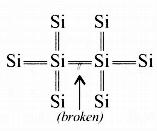
Now if one of the bonds gets broken due to some reason (collisions or high temperature) then one electron gets free and it will be having sufficient energy to cross the band gap and be ready for conduction- So in intrinsic semiconductors, current flows due to breakage of crystal bonds.
Now if one of the bonds gets broken due to some reason (collisions or high temperature) then one electron gets free and it will be having sufficient energy to cross the band gap and be ready for conduction- So in intrinsic semiconductors, current flows due to breakage of crystal bonds.
The output of a 2-input OR gate is zero only when its:- a)both inputs are 0
- b)either input is 1
- c)both inputs are 1
- d)either input is zero
Correct answer is option 'A'. Can you explain this answer?
The output of a 2-input OR gate is zero only when its:
a)
both inputs are 0
b)
either input is 1
c)
both inputs are 1
d)
either input is zero
|
|
Ritu Singh answered |
The truth table for 2-input OR gate is as shown in the figure. Thus, the output is zero only when both inputs are zero.

The diode current depends on which of the following:- a)the diode voltage, temperature, and forward saturation current
- b)only diode voltage
- c)anode voltage
- d)the diode voltage, temperature, and reverse saturation current
Correct answer is option 'D'. Can you explain this answer?
The diode current depends on which of the following:
a)
the diode voltage, temperature, and forward saturation current
b)
only diode voltage
c)
anode voltage
d)
the diode voltage, temperature, and reverse saturation current
|
|
Pooja Mehta answered |
Diodes. A diode is a discrete component that allows current to flow in one direction only. ... If the diode is put in the circuit back to front, so that the voltage at the cathode is higher than the voltage at the anode, the diode will not conduct electricity. This is called reverse bias.
In a semiconductor, current conduction is due- a)Only to holes.
- b)Only to electrons
- c)To holes and electrons
- d)None of the above
Correct answer is option 'C'. Can you explain this answer?
In a semiconductor, current conduction is due
a)
Only to holes.
b)
Only to electrons
c)
To holes and electrons
d)
None of the above
|
|
Geetika Shah answered |
There are two types of semiconductors: p-type and n-type. Therefore both holes and electrons conduct current respectively.
A photodiode is used preferably in- a)to increase voltage
- b)in forward bias condition
- c)to convert electrical energy into light
- d)in reverse bias condition
Correct answer is option 'D'. Can you explain this answer?
A photodiode is used preferably in
a)
to increase voltage
b)
in forward bias condition
c)
to convert electrical energy into light
d)
in reverse bias condition
|
|
Rohit Shah answered |
In a photo-diode when light is incident, the fractional increase in the majority carriers is much less than the fractional increase in the minority carriers. Consequently, the fractional change due to the photo-effects on the minority carrier dominated reverse bias current is more easily measurable than the fractional change due to the photo-effects on the majority carrier dominated forward bias current. Hence, photo-diodes are preferred to be used in the reverse bias condition to easily observe the variation of current with intensity.
In the binary number 10010, the MSB is- a)100
- b)0
- c)1
- d)10
Correct answer is option 'C'. Can you explain this answer?
In the binary number 10010, the MSB is
a)
100
b)
0
c)
1
d)
10

|
Sushil Kumar answered |
1001=1x23+0x22+0x21+1x20=9
For binary numbers, the digit at the extreme right is referred to as least significant bit (LSB) and the left- most digit is called the most significant bit (MSB). Hence in binary 10010, the most significant bit is 1.
For binary numbers, the digit at the extreme right is referred to as least significant bit (LSB) and the left- most digit is called the most significant bit (MSB). Hence in binary 10010, the most significant bit is 1.
For functioning of a transistor its emitter-base junction has to be:- a)Forward biased
- b)Reverse biased
- c)May be forward biased or reverse biased
- d)May not be biased at all
Correct answer is option 'A'. Can you explain this answer?
For functioning of a transistor its emitter-base junction has to be:
a)
Forward biased
b)
Reverse biased
c)
May be forward biased or reverse biased
d)
May not be biased at all
|
|
Abhijeet Ingle answered |
When emitter base junction is forward biased and collector base junction is reversed biased ,the electrons move from n to p type region and the holes moves towards the n type .When they reach other they combine enabling a current to flow across a junction.
In an n-p-n transistor, the emitter current is- a)equal to base current
- b)slightly less than the collector current
- c)slightly more than the collector current
- d)equal to the collector current
Correct answer is option 'C'. Can you explain this answer?
In an n-p-n transistor, the emitter current is
a)
equal to base current
b)
slightly less than the collector current
c)
slightly more than the collector current
d)
equal to the collector current
|
|
Sushil Kumar answered |
In the transistor circuit, the current flows from emitter to collector via base.
Ie=Ib+Ic where variables have their usual meanings.
Hence, emitter current is slightly more than the collector current.
Ie=Ib+Ic where variables have their usual meanings.
Hence, emitter current is slightly more than the collector current.

Which one of the following bonds produces asolid that reflects light in the visible region andwhose electrical conductivity decreases withtemperature and has high melting point? [2010]- a)metallic bonding
- b)van der Waal's bonding
- c)ionic bonding
- d)covalent bonding
Correct answer is option 'A'. Can you explain this answer?
Which one of the following bonds produces asolid that reflects light in the visible region andwhose electrical conductivity decreases withtemperature and has high melting point? [2010]
a)
metallic bonding
b)
van der Waal's bonding
c)
ionic bonding
d)
covalent bonding

|
Naveen Menon answered |
For a metal, conductivity decreases with
increase in temperature.
Also, metal has high melting point.
increase in temperature.
Also, metal has high melting point.


In an n-p-n transistor, the majority carriers in the emitter and collector are :- a)Free holes
- b)free electrons
- c)Free ions
- d)Valence electrons
Correct answer is option 'B'. Can you explain this answer?
In an n-p-n transistor, the majority carriers in the emitter and collector are :
a)
Free holes
b)
free electrons
c)
Free ions
d)
Valence electrons
|
|
T.ttttt answered |
Npn transistor is shown:
As we can see from the diagram, the emitter in the npn transistor is of n-type. Therefore majority charge carriers in the emitter of an npn transistor are called electrons
As we can see from the diagram, the emitter in the npn transistor is of n-type. Therefore majority charge carriers in the emitter of an npn transistor are called electrons
Which of the following is true for a forward-biased diode?- a)The anode is more positive with respect to the cathode.
- b)The anode is negative with respect to the cathode.
- c)The anode potential is equal to the cathode potential.
- d)None of the above
Correct answer is option 'A'. Can you explain this answer?
Which of the following is true for a forward-biased diode?
a)
The anode is more positive with respect to the cathode.
b)
The anode is negative with respect to the cathode.
c)
The anode potential is equal to the cathode potential.
d)
None of the above

|
Vîshåkhâ Sïñgh answered |
There are two types of ions- anions are the - ve ones & cations are the +ve ones.As you know current flow from +ve to - ve, so During electrolysis or forward biasing anions move to anodes that are +ve in nature whereas cations move to cathodes which are -ve in nature.
you can remember it by a goes to a & c goes to c.
you can remember it by a goes to a & c goes to c.
The conductivity of P – type semiconductor is due to- a)both electrons and holes
- b)holes
- c)electrons
- d)none of the above.
Correct answer is option 'B'. Can you explain this answer?
The conductivity of P – type semiconductor is due to
a)
both electrons and holes
b)
holes
c)
electrons
d)
none of the above.
|
|
Lavanya Menon answered |
A P-type semiconductor is formed when a trivalent electron deficient impurities such as boron group elements are doped with intrinsic semiconductor. As the impurities are electron deficient, they take electrons from the valence band creating a number of holes. Due this reason conductivity in P-type semiconductor is mainly due to holes rather than electrons.
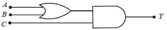
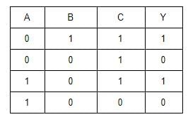
Symbolic representation of four logic gate are shown as [2011]
 Pick out which ones are for AND, NAND and NOT gates, respectively
- a)(ii), (iii) and (iv)
- b)(iii), (ii) and (i)
- c)(iii), (iii) and (iv)
- d)(ii), (iv) and (iii)
Correct answer is option 'D'. Can you explain this answer?
Symbolic representation of four logic gate are shown as [2011]
Pick out which ones are for AND, NAND and NOT gates, respectively
a)
(ii), (iii) and (iv)
b)
(iii), (ii) and (i)
c)
(iii), (iii) and (iv)
d)
(ii), (iv) and (iii)
|
|
Ayaan Madhukar answered |
Simple bro...
Correct answer is option (D)...
Correct answer is option (D)...
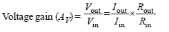
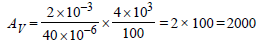
The input resistance of a silicon transistor is100 W. Base current is changed by 40 μA whichresults in a change in collector current by 2 mA.This transistor is used as a common emitteramplifier with a load resistance of 4 KΩ. Thevoltage gain of the amplifier is : [2012M]- a)2000
- b)3000
- c)4000
- d)1000
Correct answer is option 'A'. Can you explain this answer?
The input resistance of a silicon transistor is100 W. Base current is changed by 40 μA whichresults in a change in collector current by 2 mA.This transistor is used as a common emitteramplifier with a load resistance of 4 KΩ. Thevoltage gain of the amplifier is : [2012M]
a)
2000
b)
3000
c)
4000
d)
1000

|
Prasenjit Pillai answered |
Which of the statements is true for p-type semiconductors?- a)Electrons are minority carriers and pentavalent atoms are the dopants
- b)Electrons are majority carriers and trivalent atoms are the dopants
- c)Holes are minority carriers and pentavalent atoms are the dopants.
- d)Holes are majority carriers and trivalent atoms are the dopants
Correct answer is option 'D'. Can you explain this answer?
Which of the statements is true for p-type semiconductors?
a)
Electrons are minority carriers and pentavalent atoms are the dopants
b)
Electrons are majority carriers and trivalent atoms are the dopants
c)
Holes are minority carriers and pentavalent atoms are the dopants.
d)
Holes are majority carriers and trivalent atoms are the dopants
|
|
Sushil Kumar answered |
In a p-type semiconductor, the holes are the majority carriers, while the electrons are the minority carriers. A p-type semiconductor is obtained when trivalent atoms, such as aluminium, are doped in silicon atoms.
In transistors, the base region is thin and lightly doped else- a)collector current will be much larger than the emitter current
- b)the electrons or holes will not be able to reach the collector
- c)the transistor will be very thick
- d)the base current will decrease
Correct answer is option 'B'. Can you explain this answer?
In transistors, the base region is thin and lightly doped else
a)
collector current will be much larger than the emitter current
b)
the electrons or holes will not be able to reach the collector
c)
the transistor will be very thick
d)
the base current will decrease
|
|
Nikita Singh answered |
In a transistor, base bring interaction between emitter and collector. In a transistor, the base region is made very thin and lightly doped as compared to that of an emitter so that there may be less recombination of electrons and holes in this region. Due to which the base current is quite weak and the collector current is nearly equal to the emitter current.
If the base region of a transistor is doped equally to that of the emitter region, then a large electron hole recombination will take place in base, due to it, the base current would increase but collector current would decrease. Then the very purpose of a transistor would be defeated.
If the base region of a transistor is doped equally to that of the emitter region, then a large electron hole recombination will take place in base, due to it, the base current would increase but collector current would decrease. Then the very purpose of a transistor would be defeated.
A solid having uppermost energy – band partially filled with electrons is called- a)none of the above
- b)a conductor
- c)a semi – conductor
- d)an insulator
Correct answer is option 'B'. Can you explain this answer?
A solid having uppermost energy – band partially filled with electrons is called
a)
none of the above
b)
a conductor
c)
a semi – conductor
d)
an insulator
|
|
Riya Banerjee answered |
Conductor is an object or type of material that allows the flow of an electrical current in one more directions. A metal wire is a common electrical conductor. In metals such as copper or aluminium, the mobile charged particles are welcome.
An N-type Ge is obtained on doping the Ge- crystal with- a)boron
- b)gold
- c)aluminum
- d)phosphorus
Correct answer is option 'D'. Can you explain this answer?
An N-type Ge is obtained on doping the Ge- crystal with
a)
boron
b)
gold
c)
aluminum
d)
phosphorus

|
Ishani Patel answered |
Explanation:The addition of pentavalent impurities such as antimony, arsenic or phosphorous contributes free electrons, greatly increasing the conductivity of the intrinsic semiconductor.
In an unbiased p-n junction, holes diffuse from the p-region to n-region because- a)Free electrons in the n-region attract them
- b)They move across the junction by the potential difference
- c)Hole concentrate in p-region is more as compared to n-region
- d)All the above
Correct answer is option 'C'. Can you explain this answer?
In an unbiased p-n junction, holes diffuse from the p-region to n-region because
a)
Free electrons in the n-region attract them
b)
They move across the junction by the potential difference
c)
Hole concentrate in p-region is more as compared to n-region
d)
All the above
|
|
Nikita Singh answered |
The diffusion of charge carriers across a junction takes place from the region of higher concentration to the region of lower concentration. In this case, the p-region has greater concentration of holes than the n-region. Hence, in an unbiased p-n junction, holes diffuse from the p-region to the n-region.
For functioning of a transistor its collector-base junction has to be:- a)May not be biased at all
- b)Reverse biased
- c)May be forward biased or reverse biased
- d)Forward biased
Correct answer is option 'B'. Can you explain this answer?
For functioning of a transistor its collector-base junction has to be:
a)
May not be biased at all
b)
Reverse biased
c)
May be forward biased or reverse biased
d)
Forward biased
|
|
Vivek answered |
Bcoz only in that case the emitter current will pass through it almost unchanged ( I AM USING *ALMOST* BCOZ THERE IS SOME REDUCTION IN CURRENT IN THE BASE. ) If the collector-base circuit is in forward bias , it's forward current will resist the emitter current as both of them will be in opposite directions.
The efficiency of a full wave rectifier is- a)Double as that of a half wave rectifier
- b)same as that of a half wave rectifier
- c)half as that of a half wave rectifier
- d)One third as that of a half wave rectifier
Correct answer is option 'A'. Can you explain this answer?
The efficiency of a full wave rectifier is
a)
Double as that of a half wave rectifier
b)
same as that of a half wave rectifier
c)
half as that of a half wave rectifier
d)
One third as that of a half wave rectifier
|
|
Kiran Khanna answered |
Efficiency of a Full Wave Rectifier
The efficiency of a rectifier refers to how effectively it converts alternating current (AC) into direct current (DC). In the case of a full wave rectifier, it is known to have a higher efficiency compared to a half wave rectifier.
1. Half Wave Rectifier
- A half wave rectifier is a simple circuit that uses a single diode to convert AC to DC.
- It works by allowing only one half of the input AC waveform to pass through, while blocking the other half.
- The output waveform produced by a half wave rectifier is characterized by a series of positive half cycles, with the negative half cycles being eliminated.
- The rectified output waveform has a large amount of ripple and contains only half of the input power.
- Therefore, the efficiency of a half wave rectifier is relatively low.
2. Full Wave Rectifier
- A full wave rectifier is a more complex circuit that uses four diodes arranged in a bridge configuration.
- It works by allowing both halves of the input AC waveform to be rectified, resulting in a full wave rectified output waveform.
- The rectified output waveform has a smaller amount of ripple compared to a half wave rectifier, as it includes both positive and negative half cycles.
- The full wave rectifier utilizes the entire input power, resulting in a higher efficiency compared to a half wave rectifier.
3. Comparison of Efficiencies
- The efficiency of a rectifier can be defined as the ratio of the DC power output to the AC power input.
- For a half wave rectifier, the maximum efficiency is around 40.6%.
- In contrast, a full wave rectifier has a maximum efficiency of around 81.2%.
- Therefore, the efficiency of a full wave rectifier is double that of a half wave rectifier.
Conclusion
The efficiency of a full wave rectifier is double that of a half wave rectifier. This is because the full wave rectifier utilizes both halves of the input AC waveform, resulting in a higher power conversion efficiency.
Why does current flow in the forward-bias direction but not flow in the reverse-bias direction in a pn junction?- a)The anode is negative.
- b)Minority carriers are pushed to the junction.
- c)Majority carriers are pushed to the junction.
- d)The intrinsic carriers are removed.
Correct answer is option 'C'. Can you explain this answer?
Why does current flow in the forward-bias direction but not flow in the reverse-bias direction in a pn junction?
a)
The anode is negative.
b)
Minority carriers are pushed to the junction.
c)
Majority carriers are pushed to the junction.
d)
The intrinsic carriers are removed.
|
|
Pooja Mehta answered |
The PN junction has the very useful property that electrons are only able to flow in one direction. As current consists of a flow of electrons, this means that current is allowed to flow only in one direction across the structure, but it is stopped from flowing in the other direction across the junction.
A diode as a rectifier converts:- a)a.c. into d.c.
- b)varying d.c. current into constant direct current
- c)high voltage into low voltage and vice-versa
- d)d.c. into a.c.
Correct answer is option 'A'. Can you explain this answer?
A diode as a rectifier converts:
a)
a.c. into d.c.
b)
varying d.c. current into constant direct current
c)
high voltage into low voltage and vice-versa
d)
d.c. into a.c.
|
|
Sanjeevini Angadi answered |
Rectifier is a device which converts A.C into D.C.....therefore diode as a rectifier converts ac into dc
Hole is- a)An anti-particle of electron
- b)An artifically created particle
- c)Absence of free electrons
- d)A vacancy created when an electron leaves a covalent bond
Correct answer is option 'D'. Can you explain this answer?
Hole is
a)
An anti-particle of electron
b)
An artifically created particle
c)
Absence of free electrons
d)
A vacancy created when an electron leaves a covalent bond
|
|
Zeal Gosai answered |
Actually hole is not anything we just asume that when an electron moves it creates a vacancy which we call a hole.
In a p-n junction, as the diffusion process continues the width of the depletion zone- a)decreases
- b)increases
- c)remains the same
- d)oscillates
Correct answer is option 'B'. Can you explain this answer?
In a p-n junction, as the diffusion process continues the width of the depletion zone
a)
decreases
b)
increases
c)
remains the same
d)
oscillates
|
|
Preeti Iyer answered |
In reverse biasing, the positive terminal of the battery is connected to the n-type whereas the negative terminal is connected to the p-type junction. So the positive terminal tends to pull the electrons (near to the depletion layer) in n-type towards itself whereas the negative terminal pulls the holes towards itself which results in an increase in the width of the depletion layer.
When a forward bias is applied to a p-n junction, it- a)Raises the potential barrier
- b)Reduces the majority carrier current to zero
- c)Lowers the potential barrier
- d)None of the above
Correct answer is option 'C'. Can you explain this answer?
When a forward bias is applied to a p-n junction, it
a)
Raises the potential barrier
b)
Reduces the majority carrier current to zero
c)
Lowers the potential barrier
d)
None of the above
|
|
Pooja Mehta answered |
When a forward bias is applied across the p-n junction ,the applied voltage opposes the barrier voltage .
Due to it the potential barrier across the junction is lowered
Chapter doubts & questions for Semiconductor Electronics: Materials, Devices & Simple Circuits - 1 Year Dropper Course for NEET 2025 is part of NEET exam preparation. The chapters have been prepared according to the NEET exam syllabus. The Chapter doubts & questions, notes, tests & MCQs are made for NEET 2025 Exam. Find important definitions, questions, notes, meanings, examples, exercises, MCQs and online tests here.
Chapter doubts & questions of Semiconductor Electronics: Materials, Devices & Simple Circuits - 1 Year Dropper Course for NEET in English & Hindi are available as part of NEET exam.
Download more important topics, notes, lectures and mock test series for NEET Exam by signing up for free.
1 Year Dropper Course for NEET
503 videos|1698 docs|628 tests
|
|
© EduRev
|
Education Revolution
|


|


Signup on EduRev and stay on top of your study goals
10M+ students crushing their study goals daily