


All Exams >
Electronics and Communication Engineering (ECE) >
Digital Circuits >
All Questions
All questions of Semiconductor Memories: ROM, SRAM, DRAM for Electronics and Communication Engineering (ECE) Exam
Which Type of memory has a constraint of minimum operating clock frequency?- a)EEPROM
- b)Static RAM(SRAM)
- c)Dynamic RAM (DRAM)
- d)Magnetoresistive RAM(MARAM)
Correct answer is option 'C'. Can you explain this answer?
Which Type of memory has a constraint of minimum operating clock frequency?
a)
EEPROM
b)
Static RAM(SRAM)
c)
Dynamic RAM (DRAM)
d)
Magnetoresistive RAM(MARAM)

|
Imtiaz Ahmad answered |
Dynamic RAM (DRAM)
Concept:
EEPROM
EEPROM is a PROM that is that can be erased and reprogrammed using an electrical charge.
- EEPROM is a user-modifiable ROM.
- It also has a limited life - that is, the number of times it can be reprogrammed is limited to tens or hundreds of thousands of times.
- These can be programmed using special external programming signals.
- These are organized as an array of floating gate transistors.
NOTE: A special form of EEPROM is flash memory, which uses normal PC voltages for erasure and reprogramming.
SRAM
Data is stored in the transistors and requires a constant power flow.
- Because of the continuous power supply, SRAM doesn’t need to have the refreshing circuit.
- It is more expensive and holds fewer data per unit volume. So, used in cache.
- The power consumption of the SRAM is dependent on how frequently it is used.
DRAM
SDRAM (synchronous DRAM) is a generic name for various kinds of DRAM that are synchronized with the clock speed that the microprocessor is optimized for.
- The clock frequency of the microprocessor is half of the frequency of the crystal oscillator used.
- In the DRAM operation of the external pin, the interface is maintained by an externally applied clock signal.
- For DRAM continuous refreshing clock cycles are required for the retention of data stored.
MARAM
It stores the data in magnetic form instead of electric charges.
- It uses far less power than other RAMs so it is good for portable devices.
- Magnetoresistance is the tendency of a material (often ferromagnetic) to change the value of its electrical resistance in an externally-applied magnetic field.
- On account of the rising demand for fast, scalable, low power consuming, and non-volatile memory devices, especially in the automotive, enterprise storage, and aerospace and defense sectors, the global market for magnetoresistive RAM (MRAM) is likely to gain significant impetus over the forthcoming years.

Which of the following has the capability to store the information permanently?- a)RAM
- b)ROM
- c)Storage cells
- d)Both RAM and ROM
Correct answer is option 'B'. Can you explain this answer?
Which of the following has the capability to store the information permanently?
a)
RAM
b)
ROM
c)
Storage cells
d)
Both RAM and ROM
|
|
Sudhir Patel answered |
ROM (Read Only Memory) has the capability to store the information permanently. RAM provides random access to memory. Storage cells are responsible for the transfer of data from and into the memory.
Which of the following is fastest memory?- a)Secondary Memory
- b)Auxiliary Memory
- c)Cache Memory
- d)Virtual Memory
Correct answer is option 'C'. Can you explain this answer?
Which of the following is fastest memory?
a)
Secondary Memory
b)
Auxiliary Memory
c)
Cache Memory
d)
Virtual Memory
|
|
Mehul Basu answered |
Cache Memory is the fastest memory among the given options.
Cache Memory is a small, high-speed memory that is located closer to the CPU (Central Processing Unit) compared to other types of memory. It is designed to store frequently accessed data and instructions, providing fast access to the CPU. Cache memory acts as a buffer between the CPU and the main memory, reducing the time required to fetch data from the main memory.
Key Points:
- Role: Cache memory plays a crucial role in improving the performance of the computer system by reducing the average time required to access data.
- Speed: Cache memory operates at a much higher speed compared to other types of memory, such as secondary memory, auxiliary memory, and virtual memory.
- Proximity to CPU: Cache memory is located directly on the CPU chip or in close proximity to it. This closeness allows for faster access and retrieval of data and instructions.
- Size: Cache memory is relatively smaller in size compared to main memory. It is designed to hold a subset of frequently accessed data and instructions, which can be quickly retrieved by the CPU.
- Levels: Cache memory is organized into multiple levels, such as L1, L2, and L3 cache. L1 cache is the closest and fastest, while L3 cache is larger and slower.
- Cache Hierarchy: The cache hierarchy ensures that the most frequently accessed data is stored in the fastest cache level, while less frequently accessed data is stored in higher-level caches or the main memory.
- Cache Hit vs. Cache Miss: When the CPU requests data, if it is found in the cache memory, it is referred to as a cache hit, resulting in faster access. If the data is not found in the cache and needs to be retrieved from the main memory, it is referred to as a cache miss, resulting in slower access.
- Cache Coherency: Cache memory also maintains cache coherency, ensuring that multiple cache copies of the same data are synchronized and consistent.
In conclusion, cache memory is the fastest memory among the given options due to its proximity to the CPU, high-speed access, and efficient caching algorithms. It plays a critical role in improving the overall performance of the computer system.
Programmable logic array has- a)Fixed OR plane followed by a programmable AND gate
- b)Fixed AND plane followed by a programmable OR gate
- c)Programmable OR gate followed by a fixed AND gate
- d)Programmable AND gate followed by a programmable OR gate
Correct answer is option 'D'. Can you explain this answer?
Programmable logic array has
a)
Fixed OR plane followed by a programmable AND gate
b)
Fixed AND plane followed by a programmable OR gate
c)
Programmable OR gate followed by a fixed AND gate
d)
Programmable AND gate followed by a programmable OR gate
|
|
Sudhir Patel answered |
PLD’s (Programmable Logic Devices) are the circuits that contain an array of AND gates and another array of OR gates. There are three kinds of PLD’s depending upon the type of array, i.e.
- Programmable Read-Only Memory
- Programmable Array Logic
- Programmable Logic Array (PLA)
- ROM is a memory device that stores the binary information permanently.
Programmable Logic Arrays (PLA’s) implement two-level combination logic in sum-of-products (SOP) form.
PLA’s are Programmable AND array followed by Programmable OR array as shown:
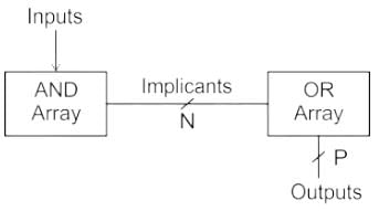
PAL: Programmable AND array followed by fixed OR array
PROM:
- It is known as programmable read-only memory
- It includes both AND array & OR array
- Out of these two arrays AND array is fixed and OR array is programmable.
VLSI chip utilizes ___________- a)NMOS
- b)CMOS
- c)BJT
- d)All of the Mentioned
Correct answer is option 'D'. Can you explain this answer?
VLSI chip utilizes ___________
a)
NMOS
b)
CMOS
c)
BJT
d)
All of the Mentioned
|
|
Sudhir Patel answered |
Very Large Scale Integration (VLSI) (ranging from 10,000 to 100,000 gates per IC) is a memory chip which is made up of NMOS, CMOS, BJT, and BiCMOS.
Since, ROM has the capability to read the information only then also it has been designed, why?- a)For controlling purpose
- b)For loading purpose
- c)For booting purpose
- d)For erasing purpose
Correct answer is option 'C'. Can you explain this answer?
Since, ROM has the capability to read the information only then also it has been designed, why?
a)
For controlling purpose
b)
For loading purpose
c)
For booting purpose
d)
For erasing purpose
|
|
Sudhir Patel answered |
ROM means “Read Only Memory”. Hence, it has capability to perform read operation only. No write or erase operation could be performed in the ROM. It has designed to provide the computer with resident programmes and for booting purpose.
Both EPROM and EEPROM are- a)Sequential access memory
- b)Random access memory
- c)Volatile memory
- d)Destructive memory
Correct answer is option 'B'. Can you explain this answer?
Both EPROM and EEPROM are
a)
Sequential access memory
b)
Random access memory
c)
Volatile memory
d)
Destructive memory
|
|
Maheshwar Das answered |
Explanation:
EPROM (Erasable Programmable Read-Only Memory) and EEPROM (Electrically Erasable Programmable Read-Only Memory) are both non-volatile memory technologies used in computer systems. However, their access methods differ.
Sequential Access Memory:
Sequential access memory refers to a type of memory where data is accessed in a sequential manner, one after the other. This means that to access a particular piece of data, all the preceding data must be read or skipped until the desired data is reached. This access method is commonly used in tape drives.
Random Access Memory:
Random access memory, on the other hand, allows for direct access to any location in memory. This means that data can be read or written to/from any memory location without the need to sequentially access the preceding data. Random access memory is commonly used in computer systems as the main memory.
Volatile Memory:
Volatile memory refers to a type of memory that loses its stored data when the power is turned off. This means that the data stored in volatile memory is temporary and needs to be saved to a non-volatile storage medium to retain it for the long term. Examples of volatile memory include RAM (Random Access Memory) and cache memory.
Destructive Memory:
Destructive memory refers to a type of memory where the act of reading or accessing the data results in its destruction or alteration. In other words, once the data is read, it cannot be recovered in its original form. This type of memory is not commonly used in computer systems.
Conclusion:
Based on the given options, the correct answer is option B, which states that EPROM and EEPROM are both random access memory. This means that data can be directly accessed from any location in EPROM and EEPROM without the need to sequentially access the preceding data. Additionally, EPROM and EEPROM are non-volatile memory technologies, which means that they retain their stored data even when the power is turned off.
The address bus width of a memory of size 1024 × 8 bits is- a)10 bits
- b)13 bits
- c)8 bits
- d)18 bits
Correct answer is option 'A'. Can you explain this answer?
The address bus width of a memory of size 1024 × 8 bits is
a)
10 bits
b)
13 bits
c)
8 bits
d)
18 bits
|
|
Arnav Roy answered |
The address bus width of a memory of size 1024 is 10 bits.
Which Type of memory has a constraint of minimum operating clock frequency?- a)EEPROM
- b)Static RAM(SRAM)
- c)Dynamic RAM (DRAM)
- d)Magnetoresistive RAM(MARAM)
Correct answer is option 'C'. Can you explain this answer?
Which Type of memory has a constraint of minimum operating clock frequency?
a)
EEPROM
b)
Static RAM(SRAM)
c)
Dynamic RAM (DRAM)
d)
Magnetoresistive RAM(MARAM)
|
|
Imtiaz Ahmad answered |
EEPROM
EEPROM is a PROM that is that can be erased and reprogrammed using an electrical charge.
EEPROM is a PROM that is that can be erased and reprogrammed using an electrical charge.
- EEPROM is a user-modifiable ROM.
- It also has a limited life - that is, the number of times it can be reprogrammed is limited to tens or hundreds of thousands of times.
- These can be programmed using special external programming signals.
- These are organized as an array of floating gate transistors.
NOTE: A special form of EEPROM is flash memory, which uses normal PC voltages for erasure and reprogramming.
SRAM
Data is stored in the transistors and requires a constant power flow.
- Because of the continuous power supply, SRAM doesn’t need to have the refreshing circuit.
- It is more expensive and holds fewer data per unit volume. So, used in cache.
- The power consumption of the SRAM is dependent on how frequently it is used.
DRAM
SDRAM (synchronous DRAM) is a generic name for various kinds of DRAM that are synchronized with the clock speed that the microprocessor is optimized for.
SDRAM (synchronous DRAM) is a generic name for various kinds of DRAM that are synchronized with the clock speed that the microprocessor is optimized for.
- The clock frequency of the microprocessor is half of the frequency of the crystal oscillator used.
- In the DRAM operation of the external pin, the interface is maintained by an externally applied clock signal.
- For DRAM continuous refreshing clock cycles are required for the retention of data stored.
MARAM
It stores the data in magnetic form instead of electric charges.
It stores the data in magnetic form instead of electric charges.
- It uses far less power than other RAMs so it is good for portable devices.
- Magnetoresistance is the tendency of a material (often ferromagnetic) to change the value of its electrical resistance in an externally-applied magnetic field.
- On account of the rising demand for fast, scalable, low power consuming, and non-volatile memory devices, especially in the automotive, enterprise storage, and aerospace and defense sectors, the global market for magnetoresistive RAM (MRAM) is likely to gain significant impetus over the forthcoming years.
Which type of ROM has to be custom built by the factory?- a)EEPROM
- b)Mask ROM
- c)EPROM
- d)PROM
Correct answer is option 'B'. Can you explain this answer?
Which type of ROM has to be custom built by the factory?
a)
EEPROM
b)
Mask ROM
c)
EPROM
d)
PROM
|
|
Sudhir Patel answered |
All types of ROM are programmable and can be programmed as per requirement but the mask ROM is always programmed for specific application and it can’t be reprogrammed. PROM stands for Programmable Read Only Memory in which the ROM can be externally programmed by the user. EPROM stands for Erasable Programmable Read Only Memory, where the ROM and be cleared and re-programmed.
Which of the following memory needs periodic refreshing?- a)SRAM
- b)DRAM
- c)Cache memory
- d)Flash memory
Correct answer is option 'B'. Can you explain this answer?
Which of the following memory needs periodic refreshing?
a)
SRAM
b)
DRAM
c)
Cache memory
d)
Flash memory
|
|
Imtiaz Ahmad answered |
To store one bit of information in our main memory we need Dram Cell which is made up of capacitor and transistor but capacitor has tendency to forget the charge or losing it’s energy to maintain that energy we required periodic Refreshing of DRAM
- Main memory is build up from DRAM chips.
- Cache memory is build up from SRAM chips.
From above explanation it is clear that DRAM is the correct answer.
PLA consists of _____.- a)Programmable AND and fixed OR arrays
- b)Programmable AND and programmable OR arrays
- c)Fixed AND and Programmable OR arrays
- d)Fixed AND and Fixed OR arrays
Correct answer is option 'B'. Can you explain this answer?
PLA consists of _____.
a)
Programmable AND and fixed OR arrays
b)
Programmable AND and programmable OR arrays
c)
Fixed AND and Programmable OR arrays
d)
Fixed AND and Fixed OR arrays
|
|
Maulik Desai answered |
PLA stands for Programmable Logic Array and it is a type of digital circuit that can be programmed to implement specific logic functions. It consists of two main components:
1. Programmable AND Array: This component consists of a matrix of AND gates, where each gate can be programmatically connected to one or more inputs. The purpose of the AND array is to generate a set of product terms based on the inputs provided.
2. Programmable OR Array: This component consists of a matrix of OR gates, where each gate can be programmatically connected to one or more product terms generated by the AND array. The purpose of the OR array is to generate the final output based on the product terms generated by the AND array.
Therefore, the correct answer to the given question is option 'B', which states that PLA consists of programmable AND and programmable OR arrays. This is because both the AND and OR arrays in a PLA are programmable, allowing for a wide range of logic functions to be implemented using a single device.
In summary, a PLA consists of programmable AND and OR arrays, which can be programmed to implement a wide range of digital logic functions.
Which bus is used for input and output in case of microprocessor operation?- a)Address bus
- b)System bus
- c)Control bus
- d)Data bus
Correct answer is option 'C'. Can you explain this answer?
Which bus is used for input and output in case of microprocessor operation?
a)
Address bus
b)
System bus
c)
Control bus
d)
Data bus
|
|
Sudhir Patel answered |
The input and output are used to control the function of a microprocessor. Hence, the control bus is used to transfer the input and output signal from microprocessor to external peripherals and or from external peripherals to microprocessor.
In a DRAM,- a)periodic refreshing is not required
- b)information is stored in a capacitor
- c)information is stored in a latch
- d)both read and write operations can be performed simultaneously
Correct answer is option 'B'. Can you explain this answer?
In a DRAM,
a)
periodic refreshing is not required
b)
information is stored in a capacitor
c)
information is stored in a latch
d)
both read and write operations can be performed simultaneously
|
|
Aryan Kulkarni answered |
Explanation:
DRAM:
DRAM stands for Dynamic Random Access Memory. It is a type of volatile memory used in computers and other electronic devices for storing and accessing data. DRAM is based on a storage cell called a capacitor, which can store a small amount of electrical charge.
Information Storage in a Capacitor:
In a DRAM, information is stored in a capacitor. Each bit of data is stored as an electrical charge in a capacitor within the memory cell. The presence or absence of charge represents the binary values 1 and 0, respectively.
Periodic Refreshing:
Unlike other types of memory, such as SRAM (Static Random Access Memory), DRAM requires periodic refreshing of its memory cells. This is because the electrical charge stored in the capacitors tends to leak away over time due to the inherent properties of the capacitor. If the charge is not refreshed, the data stored in the memory cells will be lost.
Read and Write Operations:
Both read and write operations can be performed in a DRAM. To read data from a specific memory cell, the charge stored in the capacitor is sensed and amplified, and then the data is outputted. To write data into a specific memory cell, the charge in the capacitor is changed to represent the desired data value.
Simultaneous Read and Write:
Simultaneous read and write operations are not possible in a DRAM. When a read operation is performed, the charge in the capacitor is read and the data is outputted. During a write operation, the charge in the capacitor is changed to store the desired data value. These operations cannot be performed simultaneously on the same memory cell.
Conclusion:
In conclusion, in a DRAM, information is stored in a capacitor, and periodic refreshing is required. Both read and write operations can be performed, but not simultaneously on the same memory cell.
An SRAM has address lines from A0 to A15 and data width from D0 to D7. What is the total capacity of the SRAM will be-- a)64 MB
- b)32 KB
- c)64 KB
- d)16 MB
Correct answer is option 'C'. Can you explain this answer?
An SRAM has address lines from A0 to A15 and data width from D0 to D7. What is the total capacity of the SRAM will be-
a)
64 MB
b)
32 KB
c)
64 KB
d)
16 MB
|
|
Ojas Shahane answered |
The capacity of an SRAM (Static Random Access Memory) can be calculated by multiplying the number of address lines with the data width. In this case, the SRAM has address lines from A0 to A15 and a data width from D0 to D7.
Number of address lines: A0 to A15
Number of data lines: D0 to D7
To calculate the capacity, we need to find the total number of addressable locations. This can be done by raising 2 to the power of the number of address lines. Since there are 16 address lines (A0 to A15), the total number of addressable locations is 2^16 = 65536.
The data width represents the number of bits that can be stored in each addressable location. In this case, the data width is 8 bits (D0 to D7).
Now, to find the total capacity of the SRAM, we need to multiply the number of addressable locations by the data width:
Total capacity = Number of addressable locations * Data width
Total capacity = 65536 * 8 bits
To convert the capacity to kilobytes (KB), we divide the total capacity by 1024:
Total capacity (in KB) = (65536 * 8) / 1024 = 512 KB
Therefore, the total capacity of the SRAM is 512 KB, which matches option C.
In the floppy drive, data is written to and read from the disk via a magnetic _____ head mechanism.- a)Cluster
- b)Read/Write
- c)Cylinder
- d)Recordable
Correct answer is option 'B'. Can you explain this answer?
In the floppy drive, data is written to and read from the disk via a magnetic _____ head mechanism.
a)
Cluster
b)
Read/Write
c)
Cylinder
d)
Recordable
|
|
Sudhir Patel answered |
A floppy disk is a removable disk used for storing data via magnetic facilities. In the floppy drive, data is written to and read from the disk via a magnetic read/write head mechanism.
PLDs with programmable AND and fixed OR arrays are called __________- a)PAL
- b)PLA
- c)APL
- d)PPL
Correct answer is option 'A'. Can you explain this answer?
PLDs with programmable AND and fixed OR arrays are called __________
a)
PAL
b)
PLA
c)
APL
d)
PPL
|
|
Sudhir Patel answered |
PLDs with programmable AND and fixed OR arrays are called PAL (i.e. Programmable Array Logic). However, PAL is less flexible but has higher speed.
Consider a memory chip with 24 address pins and 16 data pins. How many locations will it accommodate?- a)224
- b)224 × 16
- c)216
- d)224 × 4
Correct answer is option 'A'. Can you explain this answer?
Consider a memory chip with 24 address pins and 16 data pins. How many locations will it accommodate?
a)
224
b)
224 × 16
c)
216
d)
224 × 4
|
|
Srestha Chauhan answered |
A) 2^24 = 16,777,216
b) 2^16 = 65,536
Therefore, the memory chip will accommodate 16,777,216 locations.
b) 2^16 = 65,536
Therefore, the memory chip will accommodate 16,777,216 locations.
A given memory chip has 14 address pins and 8 data pins. It has the following number of locations.- a)28
- b)214
- c)26
- d)212
- e)222
Correct answer is option 'B'. Can you explain this answer?
A given memory chip has 14 address pins and 8 data pins. It has the following number of locations.
a)
28
b)
214
c)
26
d)
212
e)
222
|
|
Muskaan Saha answered |
Let's break down the given information and determine the number of locations in the memory chip.
- The memory chip has 14 address pins and 8 data pins.
- The number of address pins determines the number of unique addresses that can be represented.
- Each unique address corresponds to a location in the memory chip.
- The number of data pins determines the number of bits that can be stored at each location.
Determining the number of unique addresses:
- The number of address pins is 14, which means there are 2^14 (2 raised to the power of 14) unique addresses.
- This is because each address pin can have 2 possible states: 0 or 1.
- So, for each address pin, there are 2 choices, and since there are 14 address pins, the total number of unique addresses is 2^14.
Determining the number of bits per location:
- The number of data pins is 8, which means there are 8 bits that can be stored at each location.
- This is because each data pin can have 2 possible states: 0 or 1.
- So, for each data pin, there are 2 choices, and since there are 8 data pins, the total number of bits per location is 2^8.
Calculating the total number of locations:
- To determine the total number of locations in the memory chip, we multiply the number of unique addresses by the number of bits per location.
- So, the total number of locations is 2^14 * 2^8 = 2^(14+8) = 2^22 = 4,194,304.
- Therefore, the correct answer is option 'B', which states that the memory chip has 2^14 = 16,384 unique addresses and each location can store 2^8 = 256 bits.
In summary, the given memory chip has 16,384 unique addresses and each location can store 256 bits.
Which memory is difficult to interface with processor?- a)Static memory
- b)Dynamic memory
- c)ROM
- d)None of these
Correct answer is option 'B'. Can you explain this answer?
Which memory is difficult to interface with processor?
a)
Static memory
b)
Dynamic memory
c)
ROM
d)
None of these

|
Starcoders answered |
- DRAM Stores each bit of data in a separate capacitor.
- Electric charge on the capacitors slowly leaks off so data on chip would slowly be lost.
- To prevent them, DRAM refreshes periodically so due to refreshment it is difficult to interface with CPU.
- Since dynamic memory refreshes periodically so due to refreshment it is difficult to interface it.
Hence option 2 is the correct answer.
The difference between FPGA and PLD is that __________- a)FPGA is slower than PLD
- b)FPGA has high power dissipation
- c)FPGA incorporates logic blocks
- d)All of the Mentioned
Correct answer is option 'C'. Can you explain this answer?
The difference between FPGA and PLD is that __________
a)
FPGA is slower than PLD
b)
FPGA has high power dissipation
c)
FPGA incorporates logic blocks
d)
All of the Mentioned
|
|
Om Sen answered |
The Difference Between FPGA and PLD
FPGAs (Field Programmable Gate Arrays) and PLDs (Programmable Logic Devices) serve different purposes in digital circuit design. The primary distinction lies in their architecture and functionality.
FPGA Incorporates Logic Blocks
- FPGAs contain an array of configurable logic blocks (CLBs) that can be programmed to implement complex logic functions.
- These logic blocks can be interconnected in various ways to create complex digital circuits, enabling FPGAs to handle sophisticated tasks.
- The flexibility and density of logic blocks in FPGAs allow for the implementation of entire systems on a single chip.
Speed and Power Considerations
- The statement that "FPGA is slower than PLD" is generally incorrect; FPGAs can operate at high speeds, depending on their design and configuration.
- While FPGAs may have higher power dissipation compared to certain PLDs, this is not a defining characteristic that sets them apart.
Versatility and Complexity
- FPGAs are suitable for applications requiring high complexity and reconfigurability, such as digital signal processing, telecommunications, and embedded systems.
- In contrast, PLDs like PALs (Programmable Array Logic) or CPLDs (Complex Programmable Logic Devices) are typically used for simpler logic functions and are less versatile than FPGAs.
In conclusion, the correct answer is that FPGAs incorporate logic blocks, which allows them to perform complex functions and supports greater flexibility in design compared to PLDs.
ROM consist of __________- a)NOR and OR arrays
- b)NAND and NOR arrays
- c)NAND and OR arrays
- d)NOR and AND arrays
Correct answer is option 'C'. Can you explain this answer?
ROM consist of __________
a)
NOR and OR arrays
b)
NAND and NOR arrays
c)
NAND and OR arrays
d)
NOR and AND arrays
|
|
Anu Roy answered |
ROM consist of NAND and OR arrays
Explanation:
ROM stands for Read Only Memory. It is a type of computer memory that is non-volatile, meaning the stored data is retained even when the power is turned off. ROM is used to store permanent or semi-permanent data that cannot be modified or erased by normal computer operations.
Structure of ROM:
ROM consists of memory cells organized in an array. Each memory cell can store a bit of information, which is represented by a voltage level. The memory cells are connected in a matrix-like structure, with rows and columns. The intersections of the rows and columns are known as address lines, and they are used to select a particular memory cell.
ROM Array:
The ROM array is made up of two types of logic gates: NAND gates and OR gates. These gates are used to implement the desired logic functions for the ROM.
NAND Array:
The NAND array is responsible for implementing the decoding function in ROM. It takes the address inputs and generates the appropriate row select signals. The NAND gates are connected in such a way that they form a decoder, which converts the binary address inputs into a one-hot code. This one-hot code is used to select the desired row in the ROM array.
OR Array:
The OR array is responsible for implementing the data storage function in ROM. It takes the selected row from the NAND array and generates the output data. The OR gates are connected to the memory cells in each column, and they combine the outputs of the memory cells to produce the final output data.
Working:
When a specific address is given as input to the ROM, the NAND array decodes the address and selects the corresponding row. The OR array then retrieves the data from the selected row and provides it as the output.
Conclusion:
In summary, ROM consists of NAND and OR arrays. The NAND array is used for address decoding, while the OR array is used for data storage. This combination of logic gates allows ROM to store and retrieve data in a controlled and predictable manner.
How many address inputs are required to access 256 Bytes memory?- a)256
- b)2
- c)8
- d)16
Correct answer is option 'C'. Can you explain this answer?
How many address inputs are required to access 256 Bytes memory?
a)
256
b)
2
c)
8
d)
16
|
|
Saanvi Sharma answered |
Memory Organization:
To access memory, we need to provide a unique address to specify the location of the data we want to read or write. The number of address inputs required is determined by the size of the memory.
Calculation:
- 256 bytes of memory can be represented as 2^8 bytes (since 2^8 = 256).
- To address 2^8 locations, we need 8 address lines.
- Each address line can represent 2 different states (0 or 1), hence 2^8 different combinations can be made with 8 lines.
Therefore, 8 address inputs are required to access 256 Bytes memory.
In ROM, each bit is a combination of the address variables is called ___________- a)Memory unit
- b)Storage class
- c)Data word
- d)Address
Correct answer is option 'D'. Can you explain this answer?
In ROM, each bit is a combination of the address variables is called ___________
a)
Memory unit
b)
Storage class
c)
Data word
d)
Address
|
|
Sudhir Patel answered |
In ROM, each bit combination that comes out of the output lines is called data word. Usually, a word consists of 16-bits or 2-bytes.
What are the advantages of a programmable logic device (PLD) over fixed-function ICs?1. Reduction in board space requirement.2. Reduction in power requirement.3. Design security.- a)Only 1
- b)Only 2 and 3
- c)Only 1 and 3
- d)1, 2 and 3
Correct answer is option 'D'. Can you explain this answer?
What are the advantages of a programmable logic device (PLD) over fixed-function ICs?
1. Reduction in board space requirement.
2. Reduction in power requirement.
3. Design security.
a)
Only 1
b)
Only 2 and 3
c)
Only 1 and 3
d)
1, 2 and 3
|
|
Hiral Joshi answered |
Advantages of Programmable Logic Devices (PLDs) over Fixed-function ICs:
1. Reduction in board space requirement:
PLDs offer the advantage of reducing the overall board space requirement compared to fixed-function ICs. This is because PLDs are versatile and can be programmed to perform various functions, eliminating the need for multiple fixed-function ICs. By consolidating multiple functions into a single PLD, the number of ICs on the board can be significantly reduced, leading to a more compact and space-efficient design.
2. Reduction in power requirement:
Another advantage of PLDs over fixed-function ICs is the potential for reduced power consumption. Fixed-function ICs are designed to perform specific functions and may include unnecessary circuitry that is not required for a particular application. On the other hand, PLDs can be programmed to implement only the necessary logic, resulting in a more efficient use of resources and reduced power consumption. This can be particularly beneficial for battery-powered devices or applications with strict power constraints.
3. Design security:
PLDs offer enhanced design security compared to fixed-function ICs. Fixed-function ICs have their functionality hard-wired into the silicon, making it susceptible to reverse engineering and intellectual property theft. In contrast, PLDs can be programmed with custom logic designs, providing a higher level of design security. This allows designers to protect their intellectual property and prevent unauthorized replication or modification of their designs.
By combining these advantages, PLDs offer a flexible and efficient solution for a wide range of applications. They enable designers to optimize board space, reduce power consumption, and protect their designs, making them a preferred choice in many industries such as telecommunications, industrial automation, consumer electronics, and automotive.
In conclusion, the advantages of PLDs over fixed-function ICs include a reduction in board space requirement, a reduction in power requirement, and enhanced design security. These advantages make PLDs a versatile and efficient solution for various applications, offering flexibility, efficiency, and protection for designers.
Which is not a removable drive?- a)Zip
- b)Hard disk
- c)Super Disk
- d)Jaz
Correct answer is option 'C'. Can you explain this answer?
Which is not a removable drive?
a)
Zip
b)
Hard disk
c)
Super Disk
d)
Jaz
|
|
Gitanjali Banerjee answered |
Explanation:
A removable drive refers to a storage device that can be easily disconnected from a computer or any other device. It allows users to transfer data between different systems by physically removing and inserting the drive. Removable drives are typically used for data backup, file transfer, and portable storage purposes.
Zip Drive:
- A Zip drive is a type of removable storage device that was popular in the late 1990s and early 2000s.
- It uses Zip disks, which are similar in appearance to floppy disks but have a much higher storage capacity.
- Zip drives were commonly used for backing up data, storing large files, and transferring files between computers.
- They were available in various capacities, with the most common being 100MB and 250MB.
- Zip drives were connected to the computer via a parallel port, SCSI, or USB interface.
- Since Zip drives can be easily disconnected and removed from the computer, they are considered removable drives.
Hard Disk:
- A hard disk drive (HDD) is a non-removable drive that is permanently installed inside a computer or other devices.
- It is the primary storage device in most computers and is used to store the operating system, applications, and user data.
- Hard disks are not designed to be easily removed or disconnected from the computer.
- They are connected to the computer's motherboard via SATA or IDE interface cables.
- Although hard disks can be replaced or upgraded, they are not considered removable drives.
Super Disk:
- Super Disk is a high-capacity floppy disk storage system developed by Imation.
- It uses a 120MB or 240MB disk that looks similar to a regular floppy disk but has a higher storage capacity.
- Super Disk drives were compatible with standard floppy disk drives, allowing users to read and write regular floppy disks as well.
- These drives were commonly used for data backup and portable storage.
- Super Disk drives can be easily disconnected and removed from the computer, making them removable drives.
Jaz Drive:
- A Jaz drive is a removable storage solution developed by Iomega.
- It uses Jaz disks, which have a storage capacity of 1GB or 2GB.
- Jaz drives were popular in the late 1990s and early 2000s, offering a higher storage capacity than Zip drives.
- However, Jaz drives were not as widely adopted and eventually became obsolete.
- Jaz drives can be easily disconnected and removed from the computer, making them removable drives.
Conclusion:
Out of the given options, the Super Disk is a removable drive. Therefore, the correct answer is option 'C'.
Which of the following is not a part of Hard disk?- a)Platter
- b)Read/Write
- c)Valve
- d)Spindle
Correct answer is option 'C'. Can you explain this answer?
Which of the following is not a part of Hard disk?
a)
Platter
b)
Read/Write
c)
Valve
d)
Spindle

|
Sharmila Gupta answered |
Hard Disk Components
Hard disks are an essential part of modern computing systems. They are used for storing and retrieving digital data. A hard disk is composed of several components that work together to provide efficient data storage and retrieval. Let's discuss the various components of a hard disk:
1. Platter:
The platter is a circular, rigid disk made of metal or glass. It is the primary component of a hard disk and provides the surface on which data is stored. Platters are coated with a magnetic material that allows data to be written and read using the read/write head.
2. Read/Write Head:
The read/write head is responsible for reading and writing data on the platter. It is a small magnetic device that moves across the surface of the platter. When data is written to the disk, the read/write head magnetizes small areas of the platter. When data is read from the disk, the read/write head detects the magnetic fields on the platter and converts them into digital information.
3. Spindle:
The spindle is a motor that rotates the platters at a high speed. It is located at the center of the hard disk and is responsible for the rotational movement of the platters. The speed at which the platters rotate is measured in revolutions per minute (RPM) and affects the performance of the hard disk.
4. Valve (Not a Part of Hard Disk):
The option 'C' mentioned in the question, "Valve," is not a part of a hard disk. A valve is a device used to control the flow of fluids or gases. It has no relevance to the functioning of a hard disk.
In conclusion, the correct answer is option 'C,' Valve. The platter, read/write head, and spindle are the main components of a hard disk that work together to facilitate data storage and retrieval.
Why are ROMs called non-volatile memory?- a)They lose memory when power is removed
- b)They do not lose memory when power is removed
- c)They lose memory when power is supplied
- d)They do not lose memory when power is supplied
Correct answer is option 'B'. Can you explain this answer?
Why are ROMs called non-volatile memory?
a)
They lose memory when power is removed
b)
They do not lose memory when power is removed
c)
They lose memory when power is supplied
d)
They do not lose memory when power is supplied
|
|
Anand Unni answered |
Non-Volatile Memory in ROMs:
ROMs are called non-volatile memory because they do not lose memory when power is removed. This characteristic makes them different from volatile memory types like RAM.
Explanation:
Below are the key points explaining why ROMs are considered non-volatile memory:
- Retention of Data: When power is removed from a ROM, the data stored in it remains intact. This means that the information programmed into a ROM chip will not be lost even if the device is turned off. This is in contrast to volatile memory types like RAM, where data is lost when power is removed.
- Permanent Data Storage: ROMs are designed for permanent data storage. Once the data is programmed into a ROM chip during manufacturing, it cannot be easily changed or erased by the end user. This makes ROMs ideal for storing critical system software and firmware that need to remain unchanged.
- Read-Only Nature: One of the key characteristics of ROMs is their read-only nature. This means that data stored in a ROM chip can be read multiple times without the risk of losing or altering the information. This feature further reinforces the non-volatile nature of ROMs.
Conclusion:
In summary, ROMs are referred to as non-volatile memory because they retain data even when power is removed. This quality makes ROMs a reliable and secure option for storing essential data that needs to be preserved in electronic devices.
Which one of the following statement is not true for static random access memory (SRAM)- a)Static RAM stores data in the form of charge
- b)They have low capacity but offer high speed
- c)It doesn’t require periodic refreshing
- d)They are made up of six CMOS transistor
Correct answer is option 'A'. Can you explain this answer?
Which one of the following statement is not true for static random access memory (SRAM)
a)
Static RAM stores data in the form of charge
b)
They have low capacity but offer high speed
c)
It doesn’t require periodic refreshing
d)
They are made up of six CMOS transistor
|
|
Kanika Nair answered |
C) It doesn't require power to retain stored data
When both the AND and OR are programmable, such PLDs are known as __________- a)PAL
- b)PPL
- c)PLA
- d)APL
Correct answer is option 'C'. Can you explain this answer?
When both the AND and OR are programmable, such PLDs are known as __________
a)
PAL
b)
PPL
c)
PLA
d)
APL
|
|
Sudhir Patel answered |
When both the AND and OR are programmable, such PLDs are known as PLA (i.e. Programmable Logic Array). However, PLA is more flexible but has less speed.
A major disadvantage of the mask ROM is that ____________- a)It is time consuming to change the stored data when system requirements change
- b)It is very expensive to change the stored data when system requirements change
- c)It cannot be reprogrammed if stored data needs to be changed
- d)It has an extremely short life expectancy and requires frequent replacement
Correct answer is option 'C'. Can you explain this answer?
A major disadvantage of the mask ROM is that ____________
a)
It is time consuming to change the stored data when system requirements change
b)
It is very expensive to change the stored data when system requirements change
c)
It cannot be reprogrammed if stored data needs to be changed
d)
It has an extremely short life expectancy and requires frequent replacement
|
|
Sahana Dasgupta answered |
Understanding Mask ROM
Mask ROM (Read-Only Memory) is a type of non-volatile memory that is used to store permanent data. It is created during the manufacturing process, which means that the data written into it cannot be changed or modified after it is produced.
Disadvantages of Mask ROM
- Reprogramming Limitation:
- The significant disadvantage of mask ROM is that it cannot be reprogrammed. Once the data is written during the manufacturing phase, any changes to system requirements or data needs cannot be accommodated without creating a new chip.
- Cost and Time Issues:
- While options A and B discuss the expense and time-consuming nature of changing data, they are not entirely accurate regarding mask ROM. Though it's true that modifying data is costly and time-consuming, the core issue is the fundamental inability to change the data itself.
- Lifespan Misconception:
- Option D mentions life expectancy, which is misleading. Mask ROM has a long lifespan and does not require frequent replacement, unlike some other memory types.
Conclusion
In summary, the correct answer is option C because the inability to reprogram mask ROM makes it less flexible and adaptable to changes in system requirements. This limitation can lead to increased costs in the long run if system updates are necessary. Therefore, understanding the characteristics of mask ROM is crucial for making informed decisions in system design and memory allocation.
The ROM is a ___________- a)Sequential circuit
- b)Combinational circuit
- c)Magnetic circuit
- d)Static circuit
Correct answer is option 'B'. Can you explain this answer?
The ROM is a ___________
a)
Sequential circuit
b)
Combinational circuit
c)
Magnetic circuit
d)
Static circuit
|
|
Sudhir Patel answered |
ROM is a combination of different ICs. So, it is a combinational circuit. It depends on present input and not past states.
ROM has the capability to perform _____________- a)Write operation only
- b)Read operation only
- c)Both write and read operation
- d)Erase operation
Correct answer is option 'B'. Can you explain this answer?
ROM has the capability to perform _____________
a)
Write operation only
b)
Read operation only
c)
Both write and read operation
d)
Erase operation
|
|
Sudhir Patel answered |
ROM means “Read Only Memory”. Hence, it has the capability to perform read operation only. No write or erase operation could be performed in the ROM.
EPROM is generally erased by using- a)Ultraviolet rays
- b)Infrared ray
- c)12 V electrical pulse
- d)24 V electrical pulse
Correct answer is option 'A'. Can you explain this answer?
EPROM is generally erased by using
a)
Ultraviolet rays
b)
Infrared ray
c)
12 V electrical pulse
d)
24 V electrical pulse
|
|
Maulik Kapoor answered |
EPROM (Erasable Programmable Read-Only Memory) is a type of non-volatile memory that can be electrically programmed and erased for multiple times. It is widely used in various electronic devices for data storage.
EPROM Erasure Mechanism:
EPROM is generally erased using ultraviolet (UV) rays. The erasure mechanism involves the use of UV light to remove the charge that has been trapped in the floating gate transistor. The floating gate transistor is the key component of an EPROM cell, which stores the data in the form of trapped electrical charge.
Explanation:
EPROM cells are made up of MOS (Metal-Oxide-Semiconductor) transistors, which consist of a floating gate and a control gate. The floating gate is isolated from the rest of the transistor by a thin insulating oxide layer. When a voltage is applied to the control gate, the charge is stored in the floating gate, causing the transistor to be in either a programmed (charged) or erased (discharged) state.
To erase the stored data in an EPROM, it needs to be exposed to UV light. The UV light has a shorter wavelength than visible light, and it is capable of penetrating the quartz window on top of the EPROM package. The photons in the UV light have enough energy to excite the electrons in the floating gate, allowing them to escape from the oxide layer. This process is known as the Fowler-Nordheim tunneling.
The UV light exposure removes the charge from the floating gate, effectively erasing the data stored in the EPROM. Once the data is erased, the EPROM can be reprogrammed by applying the appropriate voltage to the control gate and injecting electrons into the floating gate.
Advantages of UV Erasure:
1. Non-destructive: The UV erasure process does not damage the EPROM cells, allowing them to be reprogrammed and reused.
2. Selective Erasure: UV light can erase specific EPROM cells without affecting others, allowing targeted modifications to the data.
Limitations of UV Erasure:
1. Exposure Time: The EPROM needs to be exposed to UV light for a certain duration to ensure complete erasure. This can be time-consuming compared to other erasure methods.
2. Window Requirement: EPROM packages need to have a quartz window on top to allow UV light to pass through. This adds complexity and cost to the EPROM packaging.
In conclusion, EPROM is generally erased using ultraviolet (UV) rays. The UV light removes the charge from the floating gate transistor, effectively erasing the stored data. This UV erasure process allows the EPROM to be reprogrammed and reused multiple times.
Which of the following is a non-volatile memory?- a)RAM
- b)DRAM
- c)EEPROM
- d)SRAM
Correct answer is option 'C'. Can you explain this answer?
Which of the following is a non-volatile memory?
a)
RAM
b)
DRAM
c)
EEPROM
d)
SRAM
|
|
Sudhir Patel answered |
The correct answer is Electrically Erasable Programmable Read-Only Memory (EEPROM)
- EEPROM stands for Electrically Erasable Programmable Read-Only Memory.
- It is a non-volatile memory in which the information stored Is retained even after the power goes off.
- A special type of PROM in which the information stored in it can be erased by exposing it to an electrical charge at one byte at a time.
- EEPROM generally offers excellent capabilities and performance.
- EEPROMs are constructed as arrays of floating-gate transistors.
ASIC stands for __________- a)Application Special Integrated Circuits
- b)Applied Special Integrated Circuits
- c)Application Specific Integrated Circuits
- d)Applied Specific Integrated Circuits
Correct answer is option 'C'. Can you explain this answer?
ASIC stands for __________
a)
Application Special Integrated Circuits
b)
Applied Special Integrated Circuits
c)
Application Specific Integrated Circuits
d)
Applied Specific Integrated Circuits
|
|
Sudhir Patel answered |
In digital electronics, ASIC stands for Application Specific Integrated Circuits. It is a customized integrated circuit which is produced for a specific use and not for a common-purpose.
Each NIC card is assigned a unique ________ that is burned into _________.- a)MAC address, RAM
- b)MAC address, ROM
- c)IP address, ROM
- d)IP address, RAM
Correct answer is option 'B'. Can you explain this answer?
Each NIC card is assigned a unique ________ that is burned into _________.
a)
MAC address, RAM
b)
MAC address, ROM
c)
IP address, ROM
d)
IP address, RAM
|
|
Sudhir Patel answered |
1. NIC is used to connect a computer to an Ethernet network.
2.The card usually contains the protocol control firmware and the Ethernet controller needed to support Medium Access control (MAC).
3. A MAC address is given to a network adapter. It is a hardware into the computer Network interface card (NIC) and is also unique.
4. It is a six-byte or 48-bit address that uniquely identifies the Ethernet-based connection.
For reprogrammability, PLDs use __________- a)PROM
- b)EPROM
- c)CDROM
- d)PLA
Correct answer is option 'B'. Can you explain this answer?
For reprogrammability, PLDs use __________
a)
PROM
b)
EPROM
c)
CDROM
d)
PLA
|
|
Sudhir Patel answered |
For reprogrammability, PLDs use EPROM (i.e. Erasable PROM). It erases the previous program and starts uploading a new one. However, data is erased by exposing it to UV-light, which is a tedious and time-consuming process.
The storage capacity of a SONY pen drive is 16 GB. Here what does G mean in 16 GB?- a)1024 kB
- b)1024 TB
- c)1025 PB
- d)1024 MB
Correct answer is option 'D'. Can you explain this answer?
The storage capacity of a SONY pen drive is 16 GB. Here what does G mean in 16 GB?
a)
1024 kB
b)
1024 TB
c)
1025 PB
d)
1024 MB
|
|
Sudhir Patel answered |
The conversion of memory is given below.
1 TB = 1024 GB
1 GB = 1024 MB
1 MB = 1024 kB
1 kB = 1024 Byte
1 Byte = 8 bits
The Width of a processor’s data path is measured in bits. Which of the following are common data paths?- a)8 bits
- b)12 bits
- c)16 bits
- d)32 bits
Correct answer is option 'A'. Can you explain this answer?
The Width of a processor’s data path is measured in bits. Which of the following are common data paths?
a)
8 bits
b)
12 bits
c)
16 bits
d)
32 bits
|
|
Sudhir Patel answered |
In generalised form, the data paths are of 8 bits. The data path, also known as data bus, is the channel through which the processor sends and receives data.
The programmability and high density of PLDs make them useful in the design of __________- a)ISAC
- b)ASIC
- c)SACC
- d)CISF
Correct answer is option 'B'. Can you explain this answer?
The programmability and high density of PLDs make them useful in the design of __________
a)
ISAC
b)
ASIC
c)
SACC
d)
CISF
|
|
Sudhir Patel answered |
The programmability and high density of PLDs make them useful in the design of ASIC (i.e. Application Specific Integrated Circuits) where design changes can be more rapidly and inexpensively.
If the computer has 32 k words, then this memory unit has _______ memory locations.- a)32768
- b)32769
- c)32767
- d)32000
Correct answer is option 'A'. Can you explain this answer?
If the computer has 32 k words, then this memory unit has _______ memory locations.
a)
32768
b)
32769
c)
32767
d)
32000
|
|
Sudhir Patel answered |
Concept:
1 kB = 1024 bytes
One memory location of computer occupies 1 byte of memory.
So, to occupy 32 kB of memory = 32 × 1024 = 32768 bytes are required.
∵ 1 byte = 1 memory location
∴ 32 kB memory unit of computer will require 32768 memory locations.
What does the term “random access” mean in terms of memory?- a)Any address can be accessed in systematic order
- b)Any address can be accessed in any order
- c)Addresses must be accessed in a specific order
- d)Any address can be accessed in reverse order
Correct answer is option 'B'. Can you explain this answer?
What does the term “random access” mean in terms of memory?
a)
Any address can be accessed in systematic order
b)
Any address can be accessed in any order
c)
Addresses must be accessed in a specific order
d)
Any address can be accessed in reverse order
|
|
Sudhir Patel answered |
“Random access” mean which can be accessed randomly and in other words any address can be accessed in any order.
The full form of ROM is __________- a)Read Outside Memory
- b)Read Out Memory
- c)Read Only Memory
- d)Read One Memory
Correct answer is option 'C'. Can you explain this answer?
The full form of ROM is __________
a)
Read Outside Memory
b)
Read Out Memory
c)
Read Only Memory
d)
Read One Memory
|
|
Sudhir Patel answered |
The full form of ROM is Read Only Memory.
Which ROM can be erased by an electrical signal?- a)ROM
- b)Mask ROM
- c)EPROM
- d)EEPROM
Correct answer is option 'D'. Can you explain this answer?
Which ROM can be erased by an electrical signal?
a)
ROM
b)
Mask ROM
c)
EPROM
d)
EEPROM
|
|
Sudhir Patel answered |
In EPROM (Erasable Programmable ROMs), the ROM is cleared by exposing it to UV radiation and also it’s a tedious process. Whereas, in EEPROM, the ROM can be cleared electrically and thus is less time consuming and more efficient.
The full form of EPROM is __________- a)Easy Programmable Read Only Memory
- b)Erasable Programmable Read Only Memory
- c)Eradicate Programmable Read Only Memory
- d)Easy Programmable Read Out Memory
Correct answer is option 'B'. Can you explain this answer?
The full form of EPROM is __________
a)
Easy Programmable Read Only Memory
b)
Erasable Programmable Read Only Memory
c)
Eradicate Programmable Read Only Memory
d)
Easy Programmable Read Out Memory
|
|
Sudhir Patel answered |
The full form of EPROM is Erasable Programmable Read Only Memory, where the ROM can be erased and re-used by the user.
Minimum no of MOS transistor required to make a DRAM cell is- a)1
- b)2
- c)4
- d)6
Correct answer is option 'A'. Can you explain this answer?
Minimum no of MOS transistor required to make a DRAM cell is
a)
1
b)
2
c)
4
d)
6
|
|
Starcoders answered |
In a DRAM, a capacitor is used to store a bit of data along with a MOSFET (transfer device) which acts as a switch.
The circuit is as shown:
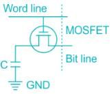
In a DRAM:
The circuit is as shown:
In a DRAM:
- Periodic refreshing is required.
- The information is stored in a capacitor.
- Both read and write operations cannot be performed simultaneously.
How many bits are in a byte?- a)2
- b)4
- c)8
- d)16
Correct answer is option 'C'. Can you explain this answer?
How many bits are in a byte?
a)
2
b)
4
c)
8
d)
16
|
|
Sudhir Patel answered |
1. A bit is the smallest unit of storage.
2. A bit stores just a 0 or 1.
3. Computers are designed to store data and execute instructions in bit multiples called bytes.
4. One byte is equal to 8 bits.
2. A bit stores just a 0 or 1.
3. Computers are designed to store data and execute instructions in bit multiples called bytes.
4. One byte is equal to 8 bits.
In ROM, each bit combination that comes out of the output lines is called ___________- a)Memory unit
- b)Storage class
- c)Data word
- d)Address
Correct answer is option 'C'. Can you explain this answer?
In ROM, each bit combination that comes out of the output lines is called ___________
a)
Memory unit
b)
Storage class
c)
Data word
d)
Address
|
|
Sudhir Patel answered |
In ROM, each bit combination that comes out of the output lines is called data word. Usually, a word consists of 16-bits or 2-bytes.
Chapter doubts & questions for Semiconductor Memories: ROM, SRAM, DRAM - Digital Circuits 2025 is part of Electronics and Communication Engineering (ECE) exam preparation. The chapters have been prepared according to the Electronics and Communication Engineering (ECE) exam syllabus. The Chapter doubts & questions, notes, tests & MCQs are made for Electronics and Communication Engineering (ECE) 2025 Exam. Find important definitions, questions, notes, meanings, examples, exercises, MCQs and online tests here.
Chapter doubts & questions of Semiconductor Memories: ROM, SRAM, DRAM - Digital Circuits in English & Hindi are available as part of Electronics and Communication Engineering (ECE) exam.
Download more important topics, notes, lectures and mock test series for Electronics and Communication Engineering (ECE) Exam by signing up for free.
Digital Circuits
76 videos|175 docs|70 tests
|
|
© EduRev
|
Education Revolution
|


|


Signup to see your scores
go up within 7 days!
Access 1000+ FREE Docs, Videos and Tests
Takes less than 10 seconds to signup