


All Exams >
Electronics and Communication Engineering (ECE) >
Digital Circuits >
All Questions
All questions of Logic Gates for Electronics and Communication Engineering (ECE) Exam
A NAND gate has —– inputs and —— outputs. - a)High input and High output
- b)none of these
- c)Low input and low output
- d)Low input and high output
Correct answer is option 'D'. Can you explain this answer?
A NAND gate has —– inputs and —— outputs.
a)
High input and High output
b)
none of these
c)
Low input and low output
d)
Low input and high output
|
|
Utkarsh Patel answered |
NAND Gate Overview
A NAND gate is a fundamental digital logic gate that produces an output which is false only when all its inputs are true. It is a combination of an AND gate followed by a NOT gate.
Input and Output Characteristics
- Inputs: A NAND gate can have two or more inputs. Commonly, it is considered with two inputs for simplicity.
- Outputs: The output of a NAND gate is binary; it can either be high (1) or low (0).
Truth Table
The behavior of a NAND gate can be understood through its truth table:
- If both inputs are High (1), the output is Low (0).
- If any one of the inputs is Low (0), the output is High (1).
Why Low Input and High Output?
- Low Input Condition: When at least one input is Low (0), the output is High (1). This characteristic is what defines the NAND operation.
- High Input Condition: Only when both inputs are High (1) does the output turn Low (0). This is the only scenario where the output does not follow the typical NAND behavior.
Conclusion
Thus, the correct answer is option 'D': Low input and high output. The NAND gate's ability to produce a high output when it receives low inputs makes it essential in various digital circuits and applications, including memory and processing units. Its versatility allows it to be used in building other logic gates and complex digital systems.

How can we use the X-NOR gate as an inverter?- a)By connecting two input terminals to logic 1 and feeding the signal to be inverted to the remaining channel
- b)By connecting one input terminal to logic 0 and feeding the signal to be inverted to the other terminal
- c)By tying all input terminal to logic 0 and feeding the system to be inverted to the other terminal
- d)By tying all but one input terminal to logic 1 and feeding the signal to be inverted to the remaining terminal
Correct answer is option 'B'. Can you explain this answer?
How can we use the X-NOR gate as an inverter?
a)
By connecting two input terminals to logic 1 and feeding the signal to be inverted to the remaining channel
b)
By connecting one input terminal to logic 0 and feeding the signal to be inverted to the other terminal
c)
By tying all input terminal to logic 0 and feeding the system to be inverted to the other terminal
d)
By tying all but one input terminal to logic 1 and feeding the signal to be inverted to the remaining terminal
|
|
Hiral Joshi answered |
Explanation:
To understand how an X-NOR gate can be used as an inverter, let's first understand the working of an X-NOR gate. An X-NOR gate is a logic gate with two or more inputs and one output. It produces a high output (1) only if all of its inputs are the same (either all 0s or all 1s).
When we connect one input terminal of an X-NOR gate to logic 0 and feed the signal to be inverted to the other terminal, the gate will produce a high output (1) only when the input signal is low (0). Conversely, when the input signal is high (1), the gate will produce a low output (0). This behavior of the X-NOR gate effectively inverts the input signal.
Steps to use an X-NOR gate as an inverter:
1. Connect one input terminal of the X-NOR gate to logic 0: This ensures that the gate produces a high output (1) only when the other input terminal is also high (1).
2. Feed the signal to be inverted to the other input terminal: This input terminal receives the signal that needs to be inverted. If the input signal is low (0), the X-NOR gate will produce a low output (0). If the input signal is high (1), the X-NOR gate will produce a high output (1).
3. Connect the output of the X-NOR gate to the desired output: The output of the X-NOR gate will be the inverted version of the input signal. You can use this output for further processing or as per your requirement.
Advantages of using an X-NOR gate as an inverter:
- Simplicity: Using an X-NOR gate as an inverter is a simple and straightforward method.
- Cost-effective: X-NOR gates are commonly available and have a lower cost compared to dedicated inverters.
- Space-saving: By utilizing an X-NOR gate as an inverter, you can save space on the circuit board by avoiding the need for a separate inverter component.
Note: It is important to choose the correct logic levels for the X-NOR gate inputs and the input signal to ensure proper inversion.
The Boolean function Y = AB + CD is to be realized using only 2 input NAND gates. The minimum number of gates required is- a)2
- b)3
- c)4
- d)5
Correct answer is option 'B'. Can you explain this answer?
The Boolean function Y = AB + CD is to be realized using only 2 input NAND gates. The minimum number of gates required is
a)
2
b)
3
c)
4
d)
5
|
|
Shraddha Yadav answered |
Explanation:
To implement the Boolean function Y = AB CD using only 2-input NAND gates, we can follow the below steps:
Step 1: Draw the truth table for the given Boolean function.
A | B | C | D | Y
--|---|---|---|--
0 | 0 | 0 | 0 | 0
0 | 0 | 0 | 1 | 0
0 | 0 | 1 | 0 | 0
0 | 0 | 1 | 1 | 0
0 | 1 | 0 | 0 | 0
0 | 1 | 0 | 1 | 0
0 | 1 | 1 | 0 | 0
0 | 1 | 1 | 1 | 0
1 | 0 | 0 | 0 | 0
1 | 0 | 0 | 1 | 0
1 | 0 | 1 | 0 | 0
1 | 0 | 1 | 1 | 0
1 | 1 | 0 | 0 | 1
1 | 1 | 0 | 1 | 0
1 | 1 | 1 | 0 | 0
1 | 1 | 1 | 1 | 1
Step 2: From the truth table, we can see that the output Y is equal to 1 only when A = 1, B = 1, C = 0, and D = 0. So, we need to implement this condition using only 2-input NAND gates.
Step 3: We can use the De Morgan's theorem to simplify the expression for Y.
Y = AB CD
= (A' + B') + (C' + D')
= [(A' + B') (C' + D')]'
Step 4: We can implement the simplified expression using 3 NAND gates as shown below.
```
A B C D
| | | |
NAND NAND NAND NAND
| | | |
NAND--NAND--NAND--|
| | | |
| | | NAND
| | | |
| | NAND---NAND
| | | |
NAND---NAND---NAND--|
| | | |
| | | NAND
| | | |
| | NAND---NAND
| | | |
NAND---NAND--NAND--|
| | | |
| | | NAND
| | | |
NAND---NAND---NAND--Y
```
Therefore, the minimum number of gates required to realize the Boolean function Y = AB CD using only 2-input NAND gates is 3. Hence, option B is the correct answer.
What is the one’s complement for the binary number 011001- a)000111
- b)100110
- c)111001
- d)110001
Correct answer is option 'B'. Can you explain this answer?
What is the one’s complement for the binary number 011001
a)
000111
b)
100110
c)
111001
d)
110001
|
|
Zara Chawla answered |
Thing that you can't live without?
Electronic circuits that operate on one or more input signals to produce standard output _______- a)Series circuits
- b)Parallel Circuits
- c)Logic Signals
- d)Logic Gates
Correct answer is option 'D'. Can you explain this answer?
Electronic circuits that operate on one or more input signals to produce standard output _______
a)
Series circuits
b)
Parallel Circuits
c)
Logic Signals
d)
Logic Gates
|
|
Vaani Malhotra answered |
Logic Gates
Logic gates are electronic circuits that operate on one or more input signals to produce a standard output. They are the building blocks of digital systems and are used to perform logical operations such as AND, OR, NOT, NAND, NOR, XOR, and XNOR.
Working Principle of Logic Gates
Logic gates work based on Boolean algebra, which is a mathematical system that deals with binary variables and logical operations. In Boolean algebra, the variables can take only two values, typically represented as 0 (false) and 1 (true). The logic gates process these binary inputs and generate binary outputs based on predefined logical operations.
Types of Logic Gates
There are several types of logic gates, each with its own unique functionality. Some of the commonly used logic gates include:
1. AND Gate: The AND gate produces a high output (logic 1) only when all of its inputs are high (logic 1).
2. OR Gate: The OR gate produces a high output (logic 1) when any of its inputs are high (logic 1).
3. NOT Gate: The NOT gate, also known as an inverter, produces the complement of its input. For example, if the input is high (logic 1), the output will be low (logic 0) and vice versa.
4. NAND Gate: The NAND gate is an AND gate followed by a NOT gate. It produces a low output (logic 0) only when all of its inputs are high (logic 1).
5. NOR Gate: The NOR gate is an OR gate followed by a NOT gate. It produces a low output (logic 0) when any of its inputs are high (logic 1).
6. XOR Gate: The XOR gate produces a high output (logic 1) when there is an odd number of high inputs.
7. XNOR Gate: The XNOR gate is an XOR gate followed by a NOT gate. It produces a high output (logic 1) when there is an even number of high inputs.
Applications of Logic Gates
Logic gates are fundamental components in digital circuits and are used in various electronic devices and systems. Some common applications of logic gates include:
1. Arithmetic circuits: Logic gates are used in arithmetic circuits such as adders, subtractors, and multipliers.
2. Memory units: Logic gates are used in memory units to store and retrieve binary information.
3. Control units: Logic gates are used in control units of computers and microprocessors to perform logical operations for instruction execution.
4. Communication systems: Logic gates are used in communication systems to encode and decode digital signals.
5. Digital displays: Logic gates are used in digital displays such as seven-segment displays to control the segments and display numbers and characters.
In conclusion, logic gates are electronic circuits that process input signals and produce standard output based on predefined logical operations. They are essential components in digital systems and have a wide range of applications in various electronic devices and systems.
Which of the following are the arithmetic logic gates?- a)X-OR
- b)X-NOR
- c)Both
- d)None
Correct answer is option 'C'. Can you explain this answer?
Which of the following are the arithmetic logic gates?
a)
X-OR
b)
X-NOR
c)
Both
d)
None
|
|
Ravi Singh answered |
X-OR and X-NOR are termed as arithmetic gates because these gates are so connected that they carry out an arithmetic action and the output they give are the digits of the result.
The input to a logic gate is A = 1100 and B = 1010. What will be the output, if the logic gate is NAND gate?- a)1101
- b)111
- c)0110
- d)1011
Correct answer is option 'B'. Can you explain this answer?
The input to a logic gate is A = 1100 and B = 1010. What will be the output, if the logic gate is NAND gate?
a)
1101
b)
111
c)
0110
d)
1011
|
|
Preethi Deshpande answered |
Problem:
The input to a logic gate is A = 1100 and B = 1010. What will be the output, if the logic gate is a NAND gate?
Solution:
1. NAND Gate:
A NAND gate is a digital logic gate that performs the operation of the logical NAND (NOT AND) operation. It produces an output that is the negation of the AND gate. In other words, it gives an output of 0 if all the inputs are 1, otherwise, it gives an output of 1.
2. Input:
The given inputs to the NAND gate are A = 1100 and B = 1010.
3. Output Calculation:
To calculate the output of the NAND gate, we need to perform the NAND operation on the given inputs.
- The NAND operation is performed by first performing the AND operation on the inputs, and then negating the output of the AND gate.
- The AND operation is performed by comparing each bit of the inputs and outputting 1 only if both bits are 1, otherwise, it outputs 0.
Let's perform the AND operation on the given inputs:
- A = 1100
- B = 1010
- AND operation: 1 AND 1 = 1, 1 AND 0 = 0, 0 AND 1 = 0, 0 AND 0 = 0
- Output of AND gate: 1000
Now, let's negate the output of the AND gate to get the output of the NAND gate:
- Negation: 1 -> 0, 0 -> 1
- Output of NAND gate: 0111
4. Answer:
The output of the NAND gate for the given inputs A = 1100 and B = 1010 is 0111.
Therefore, the correct answer is option 'B' (111).
In an all NOR gate realization of a combinational circuit all EVEN and ODD level gates behave like- a)OR and AND
- b)AND and OR
- c)OR and NOT
- d)NOR and AND
Correct answer is option 'B'. Can you explain this answer?
In an all NOR gate realization of a combinational circuit all EVEN and ODD level gates behave like
a)
OR and AND
b)
AND and OR
c)
OR and NOT
d)
NOR and AND
|
|
Sudhir Patel answered |
In an all NOR gate realization of a combinational circuit,
- All Even level gates behave like AND gate
- All Odd level gates behave like OR gate
In an all NAND gate realization of a combinational circuit,
- All Even level gates behave like OR gate
- All Odd level gates behave like AND gate
An inverter performs an operation known as- a)complementation
- b)assertion
- c)inversion
- d)both answers (a) and (c)
Correct answer is option 'C'. Can you explain this answer?
An inverter performs an operation known as
a)
complementation
b)
assertion
c)
inversion
d)
both answers (a) and (c)
|
|
Bhumi Patel answered |
An inverter performs an operation known as inversion.
In the field of electronics and digital logic, an inverter is a fundamental building block that performs the operation of inversion. In simple terms, an inverter takes an input signal and produces an output signal that is the logical complement of the input.
What is inversion?
Inversion, also known as complementation, refers to the process of changing the logical state of a signal from 0 to 1 or vice versa. In other words, if the input to an inverter is high (logic 1), the output will be low (logic 0), and if the input is low (logic 0), the output will be high (logic 1).
Working principle of an inverter:
An inverter typically consists of a transistor (usually a metal-oxide-semiconductor field-effect transistor or MOSFET) and a resistor. The input signal is connected to the gate of the transistor, while the output is taken from the drain or collector terminal. The resistor is connected between the transistor's source or emitter terminal and the ground.
When the input signal is low (logic 0), the transistor is turned off, and the output is pulled up to the supply voltage through the resistor, resulting in a high output signal (logic 1). On the other hand, when the input signal is high (logic 1), the transistor is turned on, creating a path for the current to flow from the supply voltage to the ground through the transistor and resistor. This pulls the output voltage down to a low level (logic 0).
Applications of inverters:
Inverters are widely used in various electronic systems and circuits. Some of the common applications include:
1. Digital logic circuits: Inverters are essential components in digital systems, where they are used to convert signals between different logic levels.
2. Power electronics: Inverters are used to convert DC (direct current) power to AC (alternating current) power in systems such as solar inverters, uninterruptible power supplies (UPS), and motor drives.
3. Signal processing: Inverters are used in audio amplifiers and other signal processing circuits to invert and amplify signals.
4. Communication systems: Inverters play a crucial role in modulators and demodulators used in communication systems.
In conclusion, an inverter performs the operation of inversion or complementation, which involves changing the logical state of a signal from 0 to 1 or vice versa. It is a fundamental component in electronics and finds applications in various fields including digital logic, power electronics, signal processing, and communication systems.
The basic gates are:- a)AND, NOR and NOT gate
- b)AND, OR and NOT gate
- c)AND and NOT gate
- d)OR and NOT gate
Correct answer is option 'B'. Can you explain this answer?
The basic gates are:
a)
AND, NOR and NOT gate
b)
AND, OR and NOT gate
c)
AND and NOT gate
d)
OR and NOT gate
|
|
Ravi Singh answered |
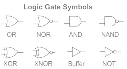
- AND, OR, NOT gates are the basic gates.
- The logic gates which are derived from the basic gates like AND, OR, NOT gates are known as derived gates. NAND, NOR, XOR, and XNOR are the derived gates.
- A universal gate is a gate which can implement any Boolean function without need to use any other gate type. The NAND and NOR gates are universal gates.
When the input to an inverter is LOW (0), the output is- a)HIGH or 0
- b)LOW or 0
- c)HIGH or 1
- d)LOW or 1
Correct answer is option 'C'. Can you explain this answer?
When the input to an inverter is LOW (0), the output is
a)
HIGH or 0
b)
LOW or 0
c)
HIGH or 1
d)
LOW or 1
|
|
Yash Patel answered |
When the input to an inverter is LOW (0), the output will be HIGH (1). Therefore, the correct answer is (c) HIGH or 1.
An inverter is a digital logic gate that performs the logical operation of negation. It takes an input signal and produces an output signal that is the logical complement of the input signal. In other words, if the input is 0, the output will be 1, and if the input is 1, the output will be 0.
Which of the following is not a logic gate?- a)AND
- b)OR
- c)IF
- d)NOT
Correct answer is option 'C'. Can you explain this answer?
Which of the following is not a logic gate?
a)
AND
b)
OR
c)
IF
d)
NOT
|
|
Sarita Yadav answered |
Different types of basic logic gates that are there include AND, OR, NOT. using these gates and making different combinations out of them, various other gates like NAND, NOR, etc are created but there is no such gate by the name of IF.
Determine the Boolean function of the following circuit.
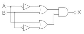
- a)X = A + B
- b)X = A̅ B̅ + A B
- c)X = A̅ B̅
- d)X = A B
Correct answer is option 'B'. Can you explain this answer?
Determine the Boolean function of the following circuit.
a)
X = A + B
b)
X = A̅ B̅ + A B
c)
X = A̅ B̅
d)
X = A B
|
|
Sudhir Patel answered |
Analysis:
Gate 1 is buffer. Input to buffer is A̅ , Output = A̅
Gate 2 is buffer. Input to buffer is B̅ , Output = B̅
Gate 3 is OR gate. Input = A̅ and B, Output = A̅ + B
Gate 4 is OR gate, Input = A and B̅ , Output = A + B̅
Gate 5 is AND gate, Input = (A̅ + B) and (A + B̅), the final output:
x = (A̅ + B) (A + B̅)
x = A̅ B̅ + A B
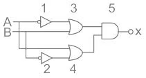
Consider the following gate network:
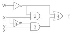
- a)Gate No. 1
- b)Gate No. 2
- c)Gate No. 3
- d)Gate No. 4
Correct answer is option 'B'. Can you explain this answer?
Consider the following gate network:
a)
Gate No. 1
b)
Gate No. 2
c)
Gate No. 3
d)
Gate No. 4
|
|
Sudhir Patel answered |
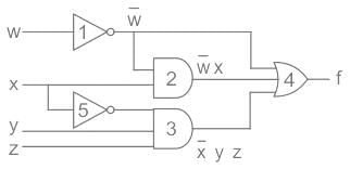
f = x̅ y z + w̅ x + w̅
= w̅ (1 + x) + x̅ y z
= w̅ + x̅ y z
∴ As the output of Gate 2 is not coming in the final simplified solution.
Gate 2 Is redundant.
Identify the logic gate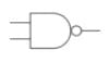
- a)AND gate
- b)OR gate
- c)NAND gate
- d)NOR gate
Correct answer is option 'C'. Can you explain this answer?
Identify the logic gate
a)
AND gate
b)
OR gate
c)
NAND gate
d)
NOR gate
|
|
Ravi Singh answered |
CONCEPT:
- Logic gate: The digital circuit that can be analysed with the help of Boolean algebra is called a logic gate or logic circuit.
- A logic gate has two or more inputs but only one output.
EXPLANATION:
- NOR gate: It is a digital circuit having two or more inputs but only one output.
- It gives a high output if either input A or B or both are low (0) otherwise it gives a high output (1).
- It is described by the Boolean expression:
- The above logic gate is the NOR gate.
Truth table for NOR gate:
Important Point
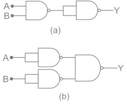 Above are the circuits that consist of NAND gates. Determine the logic operation carried out by these circuits?
- a)(a) AND gate (b) OR gate
- b)(a) NAND gate (b) OR gate
- c)(a) OR gate (b) AND gate
- d)(a) NAND gate (b) NOR gate
Correct answer is option 'A'. Can you explain this answer?
Above are the circuits that consist of NAND gates. Determine the logic operation carried out by these circuits?
a)
(a) AND gate (b) OR gate
b)
(a) NAND gate (b) OR gate
c)
(a) OR gate (b) AND gate
d)
(a) NAND gate (b) NOR gate
|
|
Sudhir Patel answered |
Circuit A:
The output X is given as;

The output Y is given as;
Circuit B:
The output P and Q are given as;
P = A̅
Q = B̅
The output Y is given as;
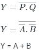
The output X is given as;
The output Y is given as;
Circuit B:
The output P and Q are given as;
P = A̅
Q = B̅
The output Y is given as;
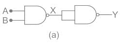
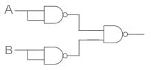
The output equivalent circuit of following circuit is
- a)INVERTER
- b)AND
- c)OR
- d)NOR
Correct answer is option 'C'. Can you explain this answer?
The output equivalent circuit of following circuit is
a)
INVERTER
b)
AND
c)
OR
d)
NOR
|
|
Sudhir Patel answered |
Concept:
De Morgans law:
The complement of the union of two sets is the intersection of their complements.
(x + y)’ = x’. y’
The complement of the intersection of two sets is the union of their complements.
(x.y)’ = x’ + y’
Analysis:
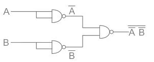
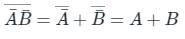
∴ OR gate
De Morgans law:
The complement of the union of two sets is the intersection of their complements.
(x + y)’ = x’. y’
The complement of the intersection of two sets is the union of their complements.
(x.y)’ = x’ + y’
Analysis:
∴ OR gate
Consider the logic circuit with input signal TEST shown in the figure. All gates in the figure shown have identical non-zero delay. The signal TEST which was at logic LOW is switched to logic HIGH and maintained at logic HIGH. The output

- a)stays HIGH throughout
- b)stays LOW throughout
- c)pulses from LOW to HIGH to LOW
- d)pulses from HIGH to LOW to HIGH
Correct answer is option 'D'. Can you explain this answer?
Consider the logic circuit with input signal TEST shown in the figure. All gates in the figure shown have identical non-zero delay. The signal TEST which was at logic LOW is switched to logic HIGH and maintained at logic HIGH. The output
a)
stays HIGH throughout
b)
stays LOW throughout
c)
pulses from LOW to HIGH to LOW
d)
pulses from HIGH to LOW to HIGH
|
|
Sudhir Patel answered |
In the given logic circuit, every gate has an identical non-zero delay.
Let the delay is t0 msec.
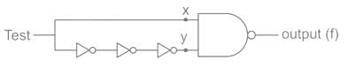
Initially test signal was at logic LOW.
⇒ x = 0, y = 1
Initially output was HIGH
Let assume test signal is switched to logic high at t = 0 m sec
At, t = 0 m sec, x = 1
As there are three NOT gates, the delay of signal to reach y input is 3t0 msec.
At, t = 3t msec, y = 0 ⇒ remains as before

NAND gate also has delay of t0 msec.
At, t = 4t0 msec, f becomes high.
At, t = 0 msec, x = 1, y = 1
At, t = 100 msec,

Output pulses from HIGH → LOW → HIGH
At, 0 < t < t0, f = HIGH
At, t0 < t < 4t0, f = LOW
At, t = 4t0, f = HIGH
Let the delay is t0 msec.
Initially test signal was at logic LOW.
⇒ x = 0, y = 1
Initially output was HIGH
Let assume test signal is switched to logic high at t = 0 m sec
At, t = 0 m sec, x = 1
As there are three NOT gates, the delay of signal to reach y input is 3t0 msec.
At, t = 3t msec, y = 0 ⇒ remains as before
NAND gate also has delay of t0 msec.
At, t = 4t0 msec, f becomes high.
At, t = 0 msec, x = 1, y = 1
At, t = 100 msec,
Output pulses from HIGH → LOW → HIGH
At, 0 < t < t0, f = HIGH
At, t0 < t < 4t0, f = LOW
At, t = 4t0, f = HIGH
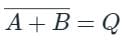
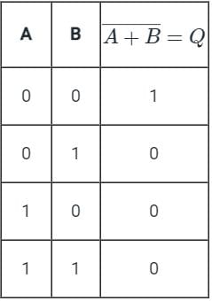
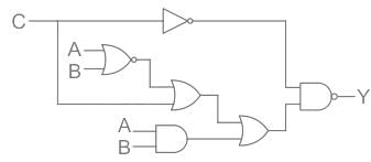
In the circuit shown in the figure, if C = 0, the expression for Y is
- a)Y = A B̅ + A̅ B
- b)Y = A + B
- c)Y = A̅ + B̅
- d)Y = A B
Correct answer is option 'A'. Can you explain this answer?
In the circuit shown in the figure, if C = 0, the expression for Y is
a)
Y = A B̅ + A̅ B
b)
Y = A + B
c)
Y = A̅ + B̅
d)
Y = A B
|
|
Sudhir Patel answered |
The given circuit is redrawn as:
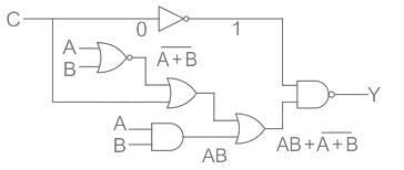
The output will be:
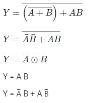
The output will be:
Chapter doubts & questions for Logic Gates - Digital Circuits 2025 is part of Electronics and Communication Engineering (ECE) exam preparation. The chapters have been prepared according to the Electronics and Communication Engineering (ECE) exam syllabus. The Chapter doubts & questions, notes, tests & MCQs are made for Electronics and Communication Engineering (ECE) 2025 Exam. Find important definitions, questions, notes, meanings, examples, exercises, MCQs and online tests here.
Chapter doubts & questions of Logic Gates - Digital Circuits in English & Hindi are available as part of Electronics and Communication Engineering (ECE) exam.
Download more important topics, notes, lectures and mock test series for Electronics and Communication Engineering (ECE) Exam by signing up for free.
Digital Circuits
76 videos|175 docs|70 tests
|
|
© EduRev
|
Education Revolution
|


|


Signup to see your scores
go up
within 7 days!
within 7 days!
Takes less than 10 seconds to signup