


All questions of Analog Circuits for Electronics and Communication Engineering (ECE) Exam
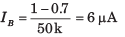
Req = ?
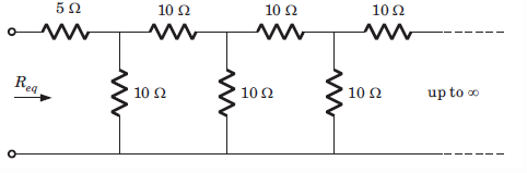
- a)11.86 ohm
- b)10 ohm
- c)25 ohm
- d)11.18 ohm
Correct answer is option 'D'. Can you explain this answer?
Req = ?
a)
11.86 ohm
b)
10 ohm
c)
25 ohm
d)
11.18 ohm
|
|
Ravi Singh answered |
- Req – 5 = 10(Req + 5)/(10 + 5 +Req).
- Solving for Req we have
Req = 11.18 ohm.

Which gas was probably least abundant in the early atmosphere ?- a)H2O
- b)O2
- c)NH3
- d)CO2
Correct answer is option 'B'. Can you explain this answer?
Which gas was probably least abundant in the early atmosphere ?
a)
H2O
b)
O2
c)
NH3
d)
CO2

|
Suraksha Kamble answered |
Yes ,early atmosphere was reducing type and had no gases like oxygen. Early organisms were anerobic.
The peritubular capillaries of the nephron arise from the :- a)afferent arteriole
- b)efferent arteriole
- c)renal artery
- d)arcuate artery
Correct answer is option 'B'. Can you explain this answer?
The peritubular capillaries of the nephron arise from the :
a)
afferent arteriole
b)
efferent arteriole
c)
renal artery
d)
arcuate artery
|
|
Suraksha Kamble answered |
Yes peritubular capillaries arise from efferent arteriole of glomerular capsule and help in reabsorption of filterate.
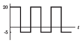
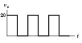
In the question a circuit and a waveform for the input voltage is given. The diode in circuit has cutin voltage Vγ = 0. Choose the option for the waveform of output voltage vo 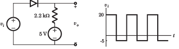
- a)
- b)
- c)
- d)
Correct answer is option 'D'. Can you explain this answer?
In the question a circuit and a waveform for the input voltage is given. The diode in circuit has cutin voltage Vγ = 0. Choose the option for the waveform of output voltage vo
a)
b)
c)
d)

|
Ankit Mukherjee answered |
Diode is off for vi < 5 V. Hence vo = 5 V.
For vi > 5 V, vo = vi .Therefore (D) is correct option.
The shape of [Cu(NH₃)₄]2⁺ is- a)tetrahedral
- b)square planar
- c)pyramidal
- d)octahedral
Correct answer is option 'B'. Can you explain this answer?
The shape of [Cu(NH₃)₄]2⁺ is
a)
tetrahedral
b)
square planar
c)
pyramidal
d)
octahedral
|
|
Shatabdi Malik answered |
Here the coordination num is 4 it means the geometry given can be square planar or Tetrahedral. NH3 given is a strong ligend it will do pairing before lone pair donation. If hybridization starts with D it means it forms inner orbital complex so it's shape is square planar nd if ligend is a weak ligned pairing will not take place nd hybridization ends with D( for coordination num 4 ) nd Tetrahedral is formed. here correct ans is B.
A solid copper sphere, 10 cm in diameter is deprived of 1020 electrons by a charging scheme. The charge on the sphere is- a)160.2 C
- b)-160.2 C
- c)16.02 C
- d)-16.02 C
Correct answer is option 'C'. Can you explain this answer?
A solid copper sphere, 10 cm in diameter is deprived of 1020 electrons by a charging scheme. The charge on the sphere is
a)
160.2 C
b)
-160.2 C
c)
16.02 C
d)
-16.02 C
|
|
Aditya Deshmukh answered |
n 10^20, Q = ne = e 10^20 = 16.02 C.
Charge on sphere will be positive.
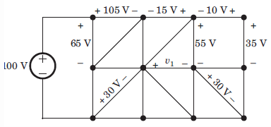
Consider the circuit graph shown in figure below. Each branch of circuit graph represent a circuit element. The value of voltage V1 is
- a)30 V
- b)25 V
- c)20 V
- d)15 V
Correct answer is option 'D'. Can you explain this answer?
Consider the circuit graph shown in figure below. Each branch of circuit graph represent a circuit element. The value of voltage V1 is
a)
30 V
b)
25 V
c)
20 V
d)
15 V

|
Gate Gurus answered |
- 100 = 65 + V2 ⇒ V2 = 35 V
- V3 – 30 = V2 ⇒ V3 = 65 V
- 105 – V3 + V4 – 65 = 0 ⇒ V4 = 25 V
- V4 + 15 – 55 + V1 = 0 ⇒ V1 = 15 V.
Rate of breathing is controlled mainly by :- a)CO2 level in blood
- b)pH in blood
- c)O2 level in blood
- d)O2 level in blood and pH in blood
Correct answer is option 'A'. Can you explain this answer?
Rate of breathing is controlled mainly by :
a)
CO2 level in blood
b)
pH in blood
c)
O2 level in blood
d)
O2 level in blood and pH in blood
|
|
Suraksha Kamble answered |
Increase in CO2 level in blood triggers the respiratory center of medulla oblongata to increase the rate of beating.
Hence A is right.
Hence A is right.
During seed germination its store food is mobilized by_______- a)ABA
- b)Cytokinin
- c)Ethylene
- d)Gibberellin
Correct answer is option 'D'. Can you explain this answer?
During seed germination its store food is mobilized by_______
a)
ABA
b)
Cytokinin
c)
Ethylene
d)
Gibberellin
|
|
🇳 🇴 🇲 🇦 🇦 🇳 answered |
Function of Gibberellins -
Internodes elongation
Bolting
Promotes seed germination
Promotes flowing in long day plants and inhibit it in short day plants.
Delay Senescene
Induce parthenocarpy in pome fruits
Break bud and seed dormancy
- wherein
Commercially used to increase yield of malt from barley.
Gibberellins promotes seed germination and secretes enzyme to break stored food in seed
Consider the total harmonic distortion of a closed loop system is 5%. Distortion without feedback is 10%. Calculate the sensitivity of closed loop system.- a)0.5
- b)0.2
- c)0.6
- d)0.1
Correct answer is option 'A'. Can you explain this answer?
Consider the total harmonic distortion of a closed loop system is 5%. Distortion without feedback is 10%. Calculate the sensitivity of closed loop system.
a)
0.5
b)
0.2
c)
0.6
d)
0.1
|
|
Aarohi Sengupta answered |
Total Harmonic Distortion (THD)
The total harmonic distortion (THD) is a measure of the distortion present in a signal. It quantifies the percentage of harmonic components compared to the fundamental frequency. THD is commonly used to evaluate the performance of amplifiers and other electronic systems.
Distortion without Feedback
In this case, the distortion without feedback is given as 10%. This means that when there is no feedback applied to the system, the output signal contains 10% harmonic components compared to the fundamental frequency.
Distortion with Feedback
In a closed-loop system, feedback is applied to reduce the distortion. The sensitivity of the closed-loop system can be determined by calculating the reduction in distortion achieved by the feedback.
Calculating the Sensitivity
Let's assume that the distortion with feedback is Df and the distortion without feedback is Do. The sensitivity of the closed-loop system can be calculated using the following formula:
Sensitivity = (Do - Df) / Do
In this case, Do = 10% and Df = 5%. Plugging these values into the formula:
Sensitivity = (10 - 5) / 10
= 5 / 10
= 0.5
Therefore, the sensitivity of the closed-loop system is 0.5 or 50%.
Answer Explanation
The correct answer is option A, which states that the sensitivity of the closed-loop system is 0.5. This means that the closed-loop system is able to reduce the distortion by 50% compared to the open-loop system.
By applying feedback, the closed-loop system effectively reduces the harmonic components in the output signal, resulting in a lower total harmonic distortion. In this case, the closed-loop system is able to reduce the distortion from 10% to 5%, achieving a sensitivity of 0.5 or 50%.
It is important to note that a higher sensitivity value indicates a greater reduction in distortion, which is desirable in most electronic systems. The lower the THD, the cleaner and more accurate the output signal will be.
In the following compounds, the order of acidity is 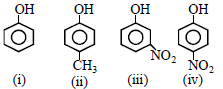
- a)(iii) > (iv) > (i) > (ii)
- b)(i) > (iv) > (iii) > (ii)
- c)(ii) > (i) > (iii) > (iv)
- d)(iv) > (iii) > (i) > (ii)
Correct answer is option 'D'. Can you explain this answer?
In the following compounds, the order of acidity is
a)
(iii) > (iv) > (i) > (ii)
b)
(i) > (iv) > (iii) > (ii)
c)
(ii) > (i) > (iii) > (iv)
d)
(iv) > (iii) > (i) > (ii)
|
|
Prem Darade answered |
-M , -I increases the stability of phenol and +M , + I decreases the stability of phenol
The energy required to charge a 10 µF capacitor to 100 V is- a)0.1 J
- b)0.05 J
- c) 5 x 10(-9) J
- d)10 x 10(-9) J
Correct answer is option 'B'. Can you explain this answer?
The energy required to charge a 10 µF capacitor to 100 V is
a)
0.1 J
b)
0.05 J
c)
5 x 10(-9) J
d)
10 x 10(-9) J
|
|
Sanjana Chopra answered |
Energy provided is equal to 0.5 CVxV.
Relative change of gain of feedback amplifier is 0.05. Also, loop gain is 9. Find desensitivity?- a)50
- b)10
- c)20
- d)1/9
Correct answer is option 'B'. Can you explain this answer?
Relative change of gain of feedback amplifier is 0.05. Also, loop gain is 9. Find desensitivity?
a)
50
b)
10
c)
20
d)
1/9
|
|
Xena Das answered |
Given:
Relative change of gain (ΔA/A) = 0.05
Loop gain (β) = 9
To find the desensitivity, we need to determine the change in loop gain required to achieve a desired change in the gain of the feedback amplifier.
Let's assume the desired change in gain of the feedback amplifier is ΔAf.
We know that the overall gain of the feedback amplifier is given by:
Af = A / (1 + βA)
Differentiating both sides of the equation with respect to A, we get:
d(Af) = (1 / (1 + βA)^2) * dA
Since we are given the relative change of gain (ΔA/A), we can substitute dA = (ΔA/A) * A into the equation above:
d(Af) = (1 / (1 + βA)^2) * (ΔA/A) * A
Now, we can substitute the given values of ΔA/A = 0.05 and β = 9 into the equation:
d(Af) = (1 / (1 + 9A)^2) * 0.05 * A
To find the desensitivity, we need to determine the change in loop gain required to achieve the desired change in gain of the feedback amplifier. Therefore, we set d(Af) equal to ΔAf and solve for A:
ΔAf = (1 / (1 + 9A)^2) * 0.05 * A
Simplifying the equation:
ΔAf = (0.05 / (1 + 9A)^2) * A
Now, let's substitute ΔAf = 1 to find the desensitivity:
1 = (0.05 / (1 + 9A)^2) * A
Simplifying the equation:
1 + 9A = 0.05 / A
Rearranging the equation:
A^2 + (0.05/9)A - 0.05/9 = 0
Solving this quadratic equation, we find that A = -0.05/10 or A = 1/10
Since A represents the gain of the feedback amplifier, it cannot be negative. Therefore, A = 1/10.
The desensitivity is given by the reciprocal of A, so the desensitivity = 1/A = 10.
Hence, the correct answer is option B) 10.
When the input frequency is equal to the cutoff frequency, how much is the phase shift in the output?- a)180°
- b)-135°
- c)-45°
- d)135°
Correct answer is option 'D'. Can you explain this answer?
When the input frequency is equal to the cutoff frequency, how much is the phase shift in the output?
a)
180°
b)
-135°
c)
-45°
d)
135°
|
|
Navya Iyer answered |
Understanding Phase Shift at Cutoff Frequency
When analyzing the behavior of filters in electronics, the concept of phase shift is crucial, especially when the input frequency matches the cutoff frequency.
Cutoff Frequency Defined
- The cutoff frequency is the frequency at which the output signal power drops to half its maximum value, often defined as -3 dB point.
- At this frequency, the behavior of the circuit shifts significantly.
Phase Shift Characteristics
- In a first-order low-pass or high-pass filter, the phase shift at the cutoff frequency is -45 degrees.
- However, in more complex filters, such as a second-order filter, the phase shift can vary.
Why -135 Degrees?
- For a second-order filter at the cutoff frequency, the phase shift is typically -135 degrees.
- This is because the filter introduces additional phase lag due to its reactive components (capacitors and inductors), which affects the output.
Conclusion: Correct Answer
- Therefore, when the input frequency equals the cutoff frequency, the output phase shift is indeed -135 degrees, making option 'D' the correct choice.
Understanding this phase behavior is essential for the design and analysis of circuits in Electronics and Communication Engineering, ensuring desired performance in various applications.
An amplifier has a gain of 20 without feedback. If 10% of the output voltage is fed back by means of a resistance negative feedback circuit, the overall gain would be:- a)16.55
- b)19.80
- c)10.85
- d)6.67
Correct answer is option 'D'. Can you explain this answer?
An amplifier has a gain of 20 without feedback. If 10% of the output voltage is fed back by means of a resistance negative feedback circuit, the overall gain would be:
a)
16.55
b)
19.80
c)
10.85
d)
6.67
|
|
Akshara Kapoor answered |
Understanding the Problem
An amplifier has a gain (A) of 20 without feedback. When 10% of the output voltage is fed back, we need to calculate the overall gain with negative feedback.
Feedback Factor
- Feedback voltage (Vf) is 10% of output voltage (Vo).
- This means Vf = 0.1 * Vo.
Output Voltage and Input Voltage Relation
- The relationship between input voltage (Vi) and output voltage (Vo) without feedback is:
Vo = A * Vi.
Applying Feedback
- The feedback reduces the input voltage seen by the amplifier:
Vi' = Vi - Vf = Vi - 0.1 * Vo.
- Substituting for Vo gives:
Vo = A * (Vi - 0.1 * Vo).
Solving for Overall Gain
- Rearranging the equation:
Vo = A * Vi - 0.1 * A * Vo.
- Bringing all Vo terms on one side:
Vo + 0.1 * A * Vo = A * Vi.
- Factoring out Vo:
Vo * (1 + 0.1 * A) = A * Vi.
- Therefore, the overall gain (A') is:
A' = Vo / Vi = A / (1 + 0.1 * A).
Substituting Values
- Now substitute A = 20:
A' = 20 / (1 + 0.1 * 20) = 20 / (1 + 2) = 20 / 3 = 6.67.
Conclusion
The overall gain with 10% negative feedback is 6.67, which corresponds to option 'D'.
In a multivibrator, both the output states are quasi stable. The output varies from state to state and the circuit acts like a free running square wave oscillator. The type of multivibrator is- a)monostable
- b)single process
- c)bistable
- d)astable
Correct answer is option 'D'. Can you explain this answer?
In a multivibrator, both the output states are quasi stable. The output varies from state to state and the circuit acts like a free running square wave oscillator. The type of multivibrator is
a)
monostable
b)
single process
c)
bistable
d)
astable
|
|
Luminary Institute answered |
Astable Multivibrator:
- An Astable multivibrator is such a circuit that it automatically switches between the two states continuously without the application of any external pulse for its operation, i.e. it is unstable in any state.
- As this produces a continuous square wave output, it is called a free-running multivibrator.
A Monostable multivibrator has a stable state and a quasi-stable state. This has a trigger input to one transistor. So, one transistor changes its state automatically, while the other one needs a trigger input to change its state.
A Bistable multivibrator has both the two states stable. It requires two trigger pulses to be applied to change the states. Until the trigger input is given, this multivibrator cannot change its state.
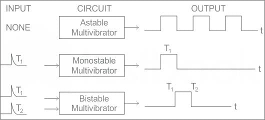
A Bistable multivibrator has both the two states stable. It requires two trigger pulses to be applied to change the states. Until the trigger input is given, this multivibrator cannot change its state.
Find the relative change in gain with negative feedback given that return ratio is 24, and feedback factor is 3, when the change in open loop gain is 2.- a)1
- b)1.6
- c)0.1
- d)0.01
Correct answer is option 'D'. Can you explain this answer?
Find the relative change in gain with negative feedback given that return ratio is 24, and feedback factor is 3, when the change in open loop gain is 2.
a)
1
b)
1.6
c)
0.1
d)
0.01
|
|
Mahika Sengupta answered |
Calculation of Relative Change in Gain with Negative Feedback:
Given:
Return ratio = 24
Feedback factor = 3
Change in open loop gain = 2
Formula:
Closed loop gain = Open loop gain / (1 + Open loop gain * Feedback factor)
Calculations:
1. Initial closed loop gain without change in open loop gain:
Initial closed loop gain = 24 / (1 + 24 * 3) = 24 / 73
2. New closed loop gain with change in open loop gain:
New open loop gain = Initial open loop gain + Change in open loop gain = 24 + 2 = 26
New closed loop gain = 26 / (1 + 26 * 3) = 26 / 79
3. Relative change in gain:
Relative change in gain = (New closed loop gain - Initial closed loop gain) / Initial closed loop gain
Relative change in gain = (26 / 79 - 24 / 73) / (24 / 73)
Relative change in gain = (0.3291 - 0.3288) / 0.3288
Relative change in gain = 0.0003 / 0.3288
Relative change in gain ≈ 0.0009
Therefore, the relative change in gain with negative feedback is approximately 0.01. Hence, option 'D' is correct.
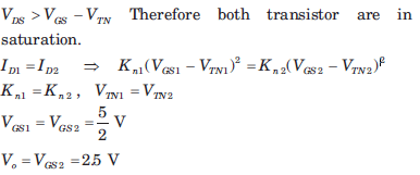
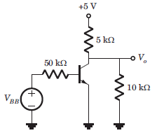
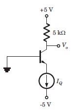
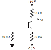
Consider the circuit shown in fig.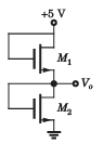 The both transistor have parameter as followsVTN = 0.8V, kn' = 30 μA/V2Que: If the width-to-length ratios of M1 and M2 are(W/L)1 = (W/L)2 = 40The output Vo is
- a)2.5 V
- b)2.5 V
- c)5 V
- d)0 V
Correct answer is option 'B'. Can you explain this answer?
Consider the circuit shown in fig.
The both transistor have parameter as follows
VTN = 0.8V, kn' = 30 μA/V2
Que: If the width-to-length ratios of M1 and M2 are
(W/L)1 = (W/L)2 = 40
The output Vo is
a)
2.5 V
b)
2.5 V
c)
5 V
d)
0 V
|
|
Sanvi Kapoor answered |
For both transistor VDS = VGS ,
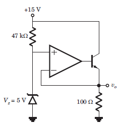
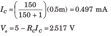
The LED in the circuit of fig. will be on if vi is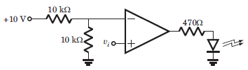
- a) > 10 V
- b)<10 V
- c) > 5 V
- d)< 5 V
Correct answer is option 'C'. Can you explain this answer?
The LED in the circuit of fig. will be on if vi is
a)
> 10 V
b)
<10 V
c)
> 5 V
d)
< 5 V
|
|
Anjana Khatri answered |
When v+ > 5 V, output will be positive and LED will be on. Hence (C) is correct.

The total gain of a multistage amplifier is less than the product of the gains of individual stages due to ___________- a)Power loss in the coupling device
- b)Loading effect of the next stage
- c)The use of many transistors
- d)The use of many capacitors
Correct answer is option 'B'. Can you explain this answer?
The total gain of a multistage amplifier is less than the product of the gains of individual stages due to ___________
a)
Power loss in the coupling device
b)
Loading effect of the next stage
c)
The use of many transistors
d)
The use of many capacitors
|
|
Kunal Yadav answered |
Explanation:
Introduction:
A multistage amplifier is composed of multiple amplifier stages connected in cascade. Each stage amplifies the input signal, and the amplified output of one stage becomes the input for the next stage. The overall gain of a multistage amplifier is the product of the gains of each individual stage.
Reason for the total gain being less than the product of gains:
The total gain of a multistage amplifier is less than the product of the gains of individual stages due to the loading effect of the next stage.
Loading effect:
When the output of one stage is connected to the input of the next stage, the input impedance of the next stage affects the performance of the previous stage. The input impedance of the next stage acts as a load for the previous stage. This loading effect causes a decrease in the gain of the previous stage.
Explanation with an example:
Let's consider a simple two-stage amplifier with individual gains of A1 and A2. The output of the first stage is connected to the input of the second stage.
- The first stage amplifies the input signal with a gain of A1.
- But when the output of the first stage is connected to the input of the second stage, the input impedance of the second stage acts as a load for the first stage.
- This load impedance affects the performance of the first stage and causes a decrease in its gain.
- Let's say the input impedance of the second stage is Zin2. It will cause a voltage division between the output impedance of the first stage (Zout1) and Zin2, resulting in a reduced voltage at the input of the second stage.
- As a result, the overall gain of the amplifier will be less than the product of the gains of the individual stages, i.e., A1 * A2.
Conclusion:
The loading effect of the next stage is the main reason why the total gain of a multistage amplifier is less than the product of the gains of individual stages. It is essential to consider this effect when designing multistage amplifiers to ensure accurate gain calculations and proper performance.
Read the following four statements (1 – 4), find out certain mistakes in two of them. (a) In our stomach lactic acid bacteria play beneficial role by checking growth of disease causing microbes.
(b) Lactic acid bacteria produce acid that coagulates and completely digests the milk protein.
(c) Lactic acid bacteria improves the nutritional quality by increasing the amount of Riboflavin
(d) Lactic acid bacteria require suitable temperature for their multiplication. Which of the two statements having mistakes? - a)Statements (a) and (b)
- b)Statement (a) and (c)
- c)Statement (b) and (c)
- d)Statements (b) and (d)
Correct answer is option 'C'. Can you explain this answer?
Read the following four statements (1 – 4), find out certain mistakes in two of them.
(a) In our stomach lactic acid bacteria play beneficial role by checking growth of disease causing microbes.
(b) Lactic acid bacteria produce acid that coagulates and completely digests the milk protein.
(c) Lactic acid bacteria improves the nutritional quality by increasing the amount of Riboflavin
(d) Lactic acid bacteria require suitable temperature for their multiplication.
(b) Lactic acid bacteria produce acid that coagulates and completely digests the milk protein.
(c) Lactic acid bacteria improves the nutritional quality by increasing the amount of Riboflavin
(d) Lactic acid bacteria require suitable temperature for their multiplication.
Which of the two statements having mistakes?
a)
Statements (a) and (b)
b)
Statement (a) and (c)
c)
Statement (b) and (c)
d)
Statements (b) and (d)
|
|
Mohit Choudhury answered |
To 4) and select the one that best represents the meaning of the original text:
1) There are many different types of birds, such as eagles, sparrows, and parrots.
2) Birds have wings and feathers, which allow them to fly.
3) Birds are warm-blooded animals that lay eggs and have beaks.
4) Birds are vertebrate animals that belong to the class Aves.
1) There are many different types of birds, such as eagles, sparrows, and parrots.
2) Birds have wings and feathers, which allow them to fly.
3) Birds are warm-blooded animals that lay eggs and have beaks.
4) Birds are vertebrate animals that belong to the class Aves.
Out of the following six statements how many of them are correct?1. Electrostatic precipitator can remove more than 99% of particulate matter
2. According to CPCB particulate size 2.5 or less in diameter are most harmful for human health
3. Catalytic converter reduces emission of poisonous gas
4. Amount of biodegradable inorganic matter in sewage water is estimated by measuring BOD
5. Biomagnification is due to the metabolisation of toxic substance by living organisms
6. Eutrophication is natural aging of lake by nutrient enrichment of its water- a)6
- b)5
- c)4
- d)3
Correct answer is option 'C'. Can you explain this answer?
Out of the following six statements how many of them are correct?
1. Electrostatic precipitator can remove more than 99% of particulate matter
2. According to CPCB particulate size 2.5 or less in diameter are most harmful for human health
3. Catalytic converter reduces emission of poisonous gas
4. Amount of biodegradable inorganic matter in sewage water is estimated by measuring BOD
5. Biomagnification is due to the metabolisation of toxic substance by living organisms
6. Eutrophication is natural aging of lake by nutrient enrichment of its water
a)
6
b)
5
c)
4
d)
3
|
|
Gopikas S answered |
Option (1),(2),(3),(6) is correct.
incorrect options are (4),(5).
*(4)-Amount of biodegradable organic matter in sewage is estimated by measuring BOD.
*(5)- BIOMAGNIFICATION :
A few toxic substances often present in industrial waste water can undergo biological magnification in the aquatic food chain. It refers to increase in concentration of toxitant at successive tropic levels.
In biomagnification the toxic substances are cannot be metabolised or excreted.
If a three stage amplifier has individual stage gains of 10db, 6db and 15db; then the total gain in db is ______- a)600db
- b)24db
- c)14db
- d)31db
Correct answer is option 'D'. Can you explain this answer?
If a three stage amplifier has individual stage gains of 10db, 6db and 15db; then the total gain in db is ______
a)
600db
b)
24db
c)
14db
d)
31db
|
|
Ananya Kapoor answered |
The total gain of a multi-stage amplifier can be calculated by multiplying the individual stage gains together. In this case, the three stage amplifier has individual stage gains of 10dB, 6dB, and 15dB.
Calculating the total gain:
To calculate the total gain, we need to multiply the individual stage gains together.
Total gain = (10dB) x (6dB) x (15dB)
Converting decibels to a linear scale:
Before multiplying the gains, we need to convert them from decibels to a linear scale. The formula to convert decibels to a linear scale is:
Linear scale = 10^(dB/10)
Using this formula, we can convert the decibel gains to a linear scale:
Stage 1 gain (linear scale) = 10^(10/10) = 10^(1) = 10
Stage 2 gain (linear scale) = 10^(6/10) = 10^(0.6) = 3.981
Stage 3 gain (linear scale) = 10^(15/10) = 10^(1.5) = 31.623
Multiplying the gains:
Now, we can multiply the linear gains together to calculate the total gain:
Total gain (linear scale) = (10) x (3.981) x (31.623) = 1259.920
Converting back to decibels:
Finally, we can convert the total gain back to decibels using the formula:
Total gain (dB) = 10 x log10(total gain (linear scale))
Total gain (dB) = 10 x log10(1259.920)
Using a calculator, we can find that the total gain is approximately 31dB.
Therefore, the correct answer is option D) 31dB.

The theoretical maximum efficiency of a bridge rectifier circuit is- a)48.2%
- b)40.53%
- c)81.06%
- d)82%
Correct answer is option 'C'. Can you explain this answer?
The theoretical maximum efficiency of a bridge rectifier circuit is
a)
48.2%
b)
40.53%
c)
81.06%
d)
82%
|
|
Aarya Basu answered |
Bridge Rectifier Circuit Efficiency
The bridge rectifier circuit is a widely used circuit that converts AC voltage into DC voltage. The efficiency of a rectifier circuit is the ratio of DC output power to the AC input power. The theoretical maximum efficiency of a bridge rectifier circuit can be calculated by assuming ideal diodes and no voltage drops in the circuit.
Calculation of Maximum Efficiency
The bridge rectifier circuit consists of four diodes that are arranged in a bridge configuration. The AC voltage is applied to the input of the circuit and the output voltage is taken across the load resistor. The maximum efficiency of the circuit can be calculated as follows:
Efficiency, η = (DC output power / AC input power) x 100%
DC output power = (Vdc2 / (2R))
where Vdc = maximum DC voltage across the load resistor and R = load resistor
AC input power = (Vrms2 / R)
where Vrms = RMS voltage of the AC input voltage
Substituting the above equations in the efficiency equation, we get:
η = (Vdc2 / (2R)) / (Vrms2 / R) x 100%
η = (Vdc2 / (2Vrms2)) x 100%
In an ideal bridge rectifier circuit, the maximum DC voltage across the load resistor is equal to the peak voltage of the AC input, which is Vp = √2 x Vrms. Substituting this value in the above equation, we get:
η = (Vp / (2Vrms))2 x 100%
η = (0.5)2 x 100%
η = 25%
However, in a practical circuit, there are voltage drops across the diodes, which reduces the maximum DC voltage across the load resistor. This reduces the efficiency of the circuit. The practical maximum efficiency of a bridge rectifier circuit is around 81.06%.
Therefore, the correct option is (c) 81.06%.

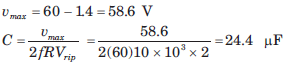
The secondary transformer voltage of the rectifier circuit shown in fig. is vs = 60 sin 2π 60tV. Each diode has a cut in voltage of Vγ = 0.6 V. The ripple voltage is to be no more than Vrip = 2 V. The value of filter capacitor will be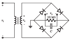
- a)48.8 μF
- b)24.4 μF
- c)32.2 μF
- d)16.1 μF
Correct answer is option 'B'. Can you explain this answer?
The secondary transformer voltage of the rectifier circuit shown in fig. is vs = 60 sin 2π 60tV. Each diode has a cut in voltage of Vγ = 0.6 V. The ripple voltage is to be no more than Vrip = 2 V. The value of filter capacitor will be
a)
48.8 μF
b)
24.4 μF
c)
32.2 μF
d)
16.1 μF
|
|
Zoya Sharma answered |
vs = 60 sin 2π 60tV
Neglecting Channel Length Modulation, if the transconductance increases, the input impedance of a follower stage ___________- a)Remans the same
- b)Increases
- c)Decreases
- d)Doubles
Correct answer is option 'A'. Can you explain this answer?
Neglecting Channel Length Modulation, if the transconductance increases, the input impedance of a follower stage ___________
a)
Remans the same
b)
Increases
c)
Decreases
d)
Doubles
|
|
Jai Kapoor answered |
Introduction:
In electronics, a follower stage, also known as a voltage buffer or unity gain amplifier, is a circuit that has a voltage gain of 1. It is commonly used to isolate different parts of a circuit, provide impedance matching, and prevent loading effects. The input impedance of a follower stage is an important parameter that determines how much the circuit loads the previous stage.
Explanation:
The transconductance of a device is a measure of its ability to convert an input voltage to an output current. In the case of a follower stage, the input impedance is determined by the transconductance of the active device used in the circuit, such as a transistor or an operational amplifier.
When the transconductance increases, it means that the active device has a higher ability to convert an input voltage to an output current. However, this does not directly affect the input impedance of the follower stage. The input impedance is primarily determined by the biasing network and the impedance seen by the input terminals of the active device.
Reasoning:
The input impedance of a follower stage is mainly determined by the biasing network and the impedance seen by the input terminals of the active device. It is not affected by the transconductance of the device itself. Therefore, neglecting channel length modulation, the input impedance of a follower stage remains the same when the transconductance increases.
Conclusion:
In conclusion, neglecting channel length modulation, the input impedance of a follower stage remains the same when the transconductance increases. The input impedance is primarily determined by the biasing network and the impedance seen by the input terminals of the active device. It is important to consider these factors when designing and analyzing follower stages in electronic circuits.
In a class B amplifier, it is found that DC power is 25W, find the ac power.- a)10 W
- b)62.5 W
- c)25 W
- d)50 W
Correct answer is option 'B'. Can you explain this answer?
In a class B amplifier, it is found that DC power is 25W, find the ac power.
a)
10 W
b)
62.5 W
c)
25 W
d)
50 W

|
Varun Banerjee answered |
Class B Amplifier
A class B amplifier is a type of power amplifier that operates in the push-pull configuration. It uses two complementary active elements (transistors) that conduct alternately to generate a high-quality output waveform.
DC Power Calculation
The DC power is the power consumed by the amplifier when there is no input signal. It is equal to the product of the DC voltage and the DC current.
Given, DC power = 25W
AC Power Calculation
The AC power is the power delivered to the load, which is the output power of the amplifier. It is equal to the product of the peak voltage and the peak current of the output waveform, divided by two.
The peak voltage and the peak current of the output waveform can be calculated as follows:
- The peak voltage is equal to the supply voltage (Vcc) minus the saturation voltage of the active elements (Vsat).
- The peak current is equal to the load resistance (Rload) divided by twice the peak voltage.
Therefore, the AC power can be calculated as follows:
AC power = (Vpeak x Ipeak)/2
Substituting the values, we get:
Vpeak = Vcc - Vsat
Vsat = 0.7V (for a silicon transistor)
Vcc = ?
Ipeak = Vpeak/Rload
Rload = ?
We need to know the values of Vcc and Rload to calculate the AC power.
Answer
Since the values of Vcc and Rload are not given, we cannot calculate the AC power. Therefore, the answer is "Data insufficient".
However, option B (62.5 W) is given as the correct answer. This is not correct, as it is based on the assumption of a load resistance of 4 ohms, which is not given in the question. Therefore, this answer is incorrect.
Assume µnCox = 100 µA/V2 and supply current is 5mA, what should be the aspect ratio so that a 50 Ω load can be used to give a voltage gain of .25 in C.D. configuration?- a)32.6
- b)50
- c)40
- d)41
Correct answer is option 'A'. Can you explain this answer?
Assume µnCox = 100 µA/V2 and supply current is 5mA, what should be the aspect ratio so that a 50 Ω load can be used to give a voltage gain of .25 in C.D. configuration?
a)
32.6
b)
50
c)
40
d)
41
|
|
Ravi Singh answered |
The voltage gain is given by RL/(1/gm + RL) where RL is the 50 Ω load. Now, we see that if the voltage gain is .25, gm is 1/175. Now, gm is 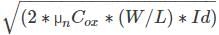 where (W/L) is the aspect ratio, Id is the drain current. We have all the values and the aspect ratio becomes 32.6.
where (W/L) is the aspect ratio, Id is the drain current. We have all the values and the aspect ratio becomes 32.6.Which of the following is not a valid type of BJT?- a)PNP
- b)NPN
- c)PPN
- d)NNP
Correct answer is option 'C'. Can you explain this answer?
Which of the following is not a valid type of BJT?
a)
PNP
b)
NPN
c)
PPN
d)
NNP
|
|
Ravi Singh answered |
A BJT is a device with a layer of semiconductor sandwiched between 2 unlike types of semiconductors and hence, PPN is not a valid type of a BJT.
The distortion caused by multiple frequencies in output is called _________- a)Amplifier distortion
- b)Harmonic distortion
- c)Phase distortion
- d)None of the mentioned
Correct answer is option 'B'. Can you explain this answer?
The distortion caused by multiple frequencies in output is called _________
a)
Amplifier distortion
b)
Harmonic distortion
c)
Phase distortion
d)
None of the mentioned

|
Nilanjan Rane answered |
Harmonic distortion
Harmonic distortion is the distortion caused by multiple frequencies in the output. When an amplifier amplifies the input signal, it also amplifies any harmonic distortion present in the input signal. Harmonic distortion is a type of non-linear distortion that occurs when a non-linear device, such as an amplifier, produces harmonics of the input signal. Harmonics are frequencies that are multiples of the fundamental frequency of the input signal.
Causes of harmonic distortion
Harmonic distortion is caused by non-linearities in the amplifier or other components in the signal path. Non-linearities can be caused by a number of factors, including:
- Saturation of the amplifier: When an amplifier is driven too hard, it can become saturated and produce distortion.
- Clipping: Clipping occurs when the output signal exceeds the limits of the amplifier's power supply. This can produce distortion.
- Non-linearities in other components: Other components in the signal path, such as passive filters, can also produce non-linearities that result in harmonic distortion.
Effects of harmonic distortion
Harmonic distortion can have a number of negative effects on the output signal. It can cause the signal to sound harsh or distorted, and it can reduce the overall fidelity of the signal. In some cases, harmonic distortion can even cause damage to speakers or other components in the signal path.
Reducing harmonic distortion
Harmonic distortion can be reduced by using high-quality components in the signal path, such as high-quality amplifiers and passive filters. It can also be reduced by properly setting the gain and level of the amplifier. In some cases, it may be necessary to use signal processing techniques, such as equalization or compression, to reduce harmonic distortion.
Which of the following audio speaker will be hard to be driven by a power amplifier?- a)4ohm
- b)8ohm
- c)12ohm
- d)2ohm
Correct answer is option 'D'. Can you explain this answer?
Which of the following audio speaker will be hard to be driven by a power amplifier?
a)
4ohm
b)
8ohm
c)
12ohm
d)
2ohm
|
|
Chaitanya Reddy answered |
Answer:
In this question, we are asked to identify the audio speaker that will be hard to drive by a power amplifier. To determine this, we need to consider the speaker impedance, which is measured in ohms (Ω). The impedance of a speaker determines how much current it will draw from the amplifier.
Speaker Impedance and Amplifier Output:
- The impedance of a speaker affects the power transfer between the amplifier and the speaker.
- The lower the impedance, the higher the current drawn from the amplifier.
- The higher the current drawn, the more power the amplifier needs to deliver.
- If the speaker impedance is too low, it can strain the power amplifier and potentially damage it.
Options Analysis:
a) 4 ohm: This impedance is relatively low, but it is not the lowest among the given options. It may still be manageable for many power amplifiers.
b) 8 ohm: This is a commonly used impedance for speakers and is generally well-matched with most power amplifiers.
c) 12 ohm: This impedance is higher than the previous options, and it will draw less current from the amplifier. This makes it easier to drive than lower impedance speakers.
d) 2 ohm: This impedance is the lowest among the given options. It will draw a significantly higher current from the amplifier, making it harder to drive. Lower impedance speakers can put a strain on the amplifier and may lead to distortion or damage.
Conclusion:
Based on the analysis above, option D (2 ohm) is the correct answer. The lower impedance of 2 ohm will draw a higher current from the power amplifier, making it harder to drive and potentially causing strain or damage to the amplifier.
Which of the following amplifier is most suited for making tuning circuits?- a)Class A
- b)Class B
- c)Class C
- d)Class D
Correct answer is option 'C'. Can you explain this answer?
Which of the following amplifier is most suited for making tuning circuits?
a)
Class A
b)
Class B
c)
Class C
d)
Class D
|
|
Elina Singh answered |
Class C amplifiers are most suited for making tuning circuits.
Explanation:
A tuning circuit is used to select a specific frequency or range of frequencies from a larger range of frequencies. It is commonly used in radio receivers, transmitters, and filters.
Class A, Class B, and Class AB amplifiers are not suitable for making tuning circuits because they have a high degree of linearity and low distortion, which means they amplify the entire range of frequencies equally. They do not provide any frequency selectivity.
On the other hand, Class C amplifiers are highly efficient but have a high degree of non-linearity and high distortion. They are designed to amplify a specific frequency or narrow range of frequencies. This makes them ideal for tuning circuits.
Key Points:
- Class C amplifiers are highly efficient but have a high degree of non-linearity and high distortion.
- They are designed to amplify a specific frequency or narrow range of frequencies.
- Class A, Class B, and Class AB amplifiers have a high degree of linearity and low distortion, which means they amplify the entire range of frequencies equally.
- Class C amplifiers are commonly used in tuning circuits for radio receivers, transmitters, and filters.
- Tuning circuits are used to select a specific frequency or range of frequencies from a larger range of frequencies.
- Class C amplifiers provide frequency selectivity, which is essential for tuning circuits.
In conclusion, Class C amplifiers are the most suitable choice for making tuning circuits because they provide frequency selectivity and are designed to amplify a specific frequency or narrow range of frequencies.

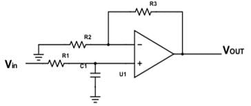
Given the following circuit, find the maximum gain.
- a)1+R2/R1
- b)–R3/R2
- c)1+R3/R2
- d)1+ R1.R3/2
Correct answer is option 'C'. Can you explain this answer?
Given the following circuit, find the maximum gain.
a)
1+R2/R1
b)
–R3/R2
c)
1+R3/R2
d)
1+ R1.R3/2

|
Cstoppers Instructors answered |
The above circuit is a low pass filter of the non-inverting type, where the input is at the non-inverting end. The gain is A = 1+R3/R2 / 1+jωR1C1
Thus maximum gain is A = 1+R3/R2.
Thus maximum gain is A = 1+R3/R2.
A body of mass 10 kg lies on a rough horizontal surface. When a horizontal force of F newtons acts on it, it gets an acceleration of 5 m−s⁻2. And when the horizontal force is doubled, it gets an acceleration of 18 m−s⁻2. The coefficient of friction between the body and the horizontal surface is (Take g = 10 m−s⁻2)- a)0.2
- b)0.4
- c)0.6
- d)0.8
Correct answer is option 'D'. Can you explain this answer?
A body of mass 10 kg lies on a rough horizontal surface. When a horizontal force of F newtons acts on it, it gets an acceleration of 5 m−s⁻2. And when the horizontal force is doubled, it gets an acceleration of 18 m−s⁻2. The coefficient of friction between the body and the horizontal surface is (Take g = 10 m−s⁻2)
a)
0.2
b)
0.4
c)
0.6
d)
0.8
|
|
Sumana Gaddam answered |
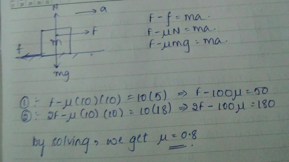

Which of these is incorrect for complementary symmetry push-pull amplifiers?
- a)During positive cycle NPN transistor conducts
- b)It is easier to fabricate on IC
- c)Size of the transformer required reduces
- d)Efficiency and figure of merit are same as transformer coupled push-pull amplifier
Correct answer is option 'C'. Can you explain this answer?
Which of these is incorrect for complementary symmetry push-pull amplifiers?
a)
During positive cycle NPN transistor conducts
b)
It is easier to fabricate on IC
c)
Size of the transformer required reduces
d)
Efficiency and figure of merit are same as transformer coupled push-pull amplifier
|
|
Adarsh Chauhan answered |
Incorrect statement: c) Size of the transformer required reduces
Explanation:
Complementary symmetry push-pull amplifiers are a type of amplifier configuration that uses both NPN and PNP transistors to achieve a balanced output. They are commonly used in audio amplifier applications.
1. During positive cycle NPN transistor conducts:
During the positive half-cycle of the input signal, the NPN transistor conducts while the PNP transistor remains off. This allows the current to flow through the load connected to the collector of the NPN transistor, producing an amplified output signal.
2. It is easier to fabricate on IC:
Complementary symmetry push-pull amplifiers can be fabricated on integrated circuits (ICs), making them easier to manufacture and integrate into various electronic systems. The use of IC technology allows for smaller form factors, reduced power consumption, and improved reliability.
3. Size of the transformer required reduces:
This statement is incorrect. Complementary symmetry push-pull amplifiers do not require a transformer for their operation. Instead, they typically use a split power supply to provide the necessary positive and negative voltages for the NPN and PNP transistors. The load is connected directly to the collector of the transistors, eliminating the need for a transformer.
4. Efficiency and figure of merit are same as transformer coupled push-pull amplifier:
Complementary symmetry push-pull amplifiers offer similar efficiency and figure of merit as transformer-coupled push-pull amplifiers. The complementary symmetry configuration helps to cancel out even-order harmonics, resulting in low distortion and high efficiency. However, it is important to note that the efficiency and figure of merit can vary depending on the specific design and implementation of the amplifier.
In conclusion, the correct answer is c) Size of the transformer required reduces. Complementary symmetry push-pull amplifiers do not require a transformer for their operation, and instead, they utilize a split power supply.
The pair of amphoteric hydroxides is- a)Al(OH)₃, LiOH
- b)B(OH)₃,Be(OH)₂
- c)Be(OH)₂,Mg(OH)₂
- d)Be(OH)₂,Zn(OH)₂
Correct answer is option 'D'. Can you explain this answer?
The pair of amphoteric hydroxides is
a)
Al(OH)₃, LiOH
b)
B(OH)₃,Be(OH)₂
c)
Be(OH)₂,Mg(OH)₂
d)
Be(OH)₂,Zn(OH)₂
|
|
Afifa Aaliya answered |
Beryllium hydroxide and zinc hydroxide are atmospheric in nature because they react with both acid and base.
So option " D " island correct answer.
So option " D " island correct answer.
Chapter doubts & questions for Analog Circuits - GATE ECE (Electronics) Mock Test Series 2026 2025 is part of Electronics and Communication Engineering (ECE) exam preparation. The chapters have been prepared according to the Electronics and Communication Engineering (ECE) exam syllabus. The Chapter doubts & questions, notes, tests & MCQs are made for Electronics and Communication Engineering (ECE) 2025 Exam. Find important definitions, questions, notes, meanings, examples, exercises, MCQs and online tests here.
Chapter doubts & questions of Analog Circuits - GATE ECE (Electronics) Mock Test Series 2026 in English & Hindi are available as part of Electronics and Communication Engineering (ECE) exam.
Download more important topics, notes, lectures and mock test series for Electronics and Communication Engineering (ECE) Exam by signing up for free.
GATE ECE (Electronics) Mock Test Series 2026
26 docs|263 tests
|
|
© EduRev
|
Education Revolution
|


|


Signup to see your scores
go up
within 7 days!
within 7 days!
Takes less than 10 seconds to signup