Electronics and Communication Engineering (ECE) Exam > Electronics and Communication Engineering (ECE) Questions > Population inversion in semiconductor laser d...
Start Learning for Free
Population inversion in semiconductor laser diode is achieved by:
- a)Lightly doping p and n sides
- b)Introducing trap centres on p and n sides
- c)Heavily doping p and n sides
- d)Reverse biasing the junction
Correct answer is option 'B'. Can you explain this answer?
| FREE This question is part of | Download PDF Attempt this Test |
Most Upvoted Answer
Population inversion in semiconductor laser diode is achieved by:a)Lig...
Population Inversion in Semiconductor Laser Diode
Introduction
In order to understand how population inversion is achieved in a semiconductor laser diode, it is important to first understand the concept of population inversion itself. Population inversion refers to the situation where the number of electrons in an excited state is greater than the number of electrons in the ground state. This is a crucial condition for the operation of a laser.
Light Amplification Process
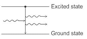
In a laser, the light amplification process occurs due to stimulated emission. Stimulated emission is a process in which an electron in an excited state is stimulated by an incoming photon to emit a second photon that is identical to the incoming photon in terms of frequency, phase, and polarization. This results in the amplification of light.
Achieving Population Inversion
To achieve population inversion in a semiconductor laser diode, the following factors need to be considered:
1. Lightly doping p and n sides:
Light doping of the p and n sides of the diode helps in achieving population inversion. This is because lightly doped semiconductors have a smaller number of impurity atoms, which leads to a lower density of energy states within the bandgap. This, in turn, reduces the probability of non-radiative recombination processes, which can hinder population inversion.
2. Introducing trap centers on p and n sides:
The introduction of trap centers on the p and n sides of the diode is another method to achieve population inversion. Trap centers are impurity atoms that create localized energy states within the bandgap. These trap states act as intermediate energy levels, allowing electrons to populate the excited state and remain there for a longer duration. This increases the probability of stimulated emission and helps in achieving population inversion.
3. Heavily doping p and n sides:
Contrary to the correct answer provided, heavily doping the p and n sides of the diode is not the preferred method to achieve population inversion. This is because heavily doped semiconductors have a higher density of impurity atoms, resulting in a higher density of energy states within the bandgap. This increases the probability of non-radiative recombination processes, which can lead to a decrease in the population inversion.
4. Reverse biasing the junction:
While reverse biasing the junction is important for the proper operation of a semiconductor laser diode, it is not directly responsible for achieving population inversion. Reverse biasing helps in creating a favorable electric field across the junction, which facilitates the injection of electrons and holes into the active region of the diode.
Conclusion
In conclusion, population inversion in a semiconductor laser diode is achieved by lightly doping the p and n sides of the diode and introducing trap centers on these sides. These methods help in reducing non-radiative recombination processes and increasing the probability of stimulated emission, thereby achieving the desired population inversion.
Free Test
FREE
| Start Free Test |
Community Answer
Population inversion in semiconductor laser diode is achieved by:a)Lig...
Concept:
What is population inversion:
“When more atoms exist in higher energy state compare to lower energy state”.
“When more atoms exist in higher energy state compare to lower energy state”.
# What is need of population inversion in LASER.
“To perform stimulated emission”
“To perform stimulated emission”
# What is stimulated emission ?
“When on atom in excited state return to the ground state in the presence of photon by emitting another photon which is identical to it in frequency, direction, polarization and phase.
“When on atom in excited state return to the ground state in the presence of photon by emitting another photon which is identical to it in frequency, direction, polarization and phase.

# How the population inversion in semiconductor cases diode occurs?
“By introduction of trap centres on P and n sides”.
“By introduction of trap centres on P and n sides”.
Attention Electronics and Communication Engineering (ECE) Students!
To make sure you are not studying endlessly, EduRev has designed Electronics and Communication Engineering (ECE) study material, with Structured Courses, Videos, & Test Series. Plus get personalized analysis, doubt solving and improvement plans to achieve a great score in Electronics and Communication Engineering (ECE).

|
Explore Courses for Electronics and Communication Engineering (ECE) exam
|

|
Similar Electronics and Communication Engineering (ECE) Doubts
Population inversion in semiconductor laser diode is achieved by:a)Lightly doping p and n sidesb)Introducing trap centres on p and n sidesc)Heavily doping p and n sidesd)Reverse biasing the junctionCorrect answer is option 'B'. Can you explain this answer?
Question Description
Population inversion in semiconductor laser diode is achieved by:a)Lightly doping p and n sidesb)Introducing trap centres on p and n sidesc)Heavily doping p and n sidesd)Reverse biasing the junctionCorrect answer is option 'B'. Can you explain this answer? for Electronics and Communication Engineering (ECE) 2024 is part of Electronics and Communication Engineering (ECE) preparation. The Question and answers have been prepared according to the Electronics and Communication Engineering (ECE) exam syllabus. Information about Population inversion in semiconductor laser diode is achieved by:a)Lightly doping p and n sidesb)Introducing trap centres on p and n sidesc)Heavily doping p and n sidesd)Reverse biasing the junctionCorrect answer is option 'B'. Can you explain this answer? covers all topics & solutions for Electronics and Communication Engineering (ECE) 2024 Exam. Find important definitions, questions, meanings, examples, exercises and tests below for Population inversion in semiconductor laser diode is achieved by:a)Lightly doping p and n sidesb)Introducing trap centres on p and n sidesc)Heavily doping p and n sidesd)Reverse biasing the junctionCorrect answer is option 'B'. Can you explain this answer?.
Population inversion in semiconductor laser diode is achieved by:a)Lightly doping p and n sidesb)Introducing trap centres on p and n sidesc)Heavily doping p and n sidesd)Reverse biasing the junctionCorrect answer is option 'B'. Can you explain this answer? for Electronics and Communication Engineering (ECE) 2024 is part of Electronics and Communication Engineering (ECE) preparation. The Question and answers have been prepared according to the Electronics and Communication Engineering (ECE) exam syllabus. Information about Population inversion in semiconductor laser diode is achieved by:a)Lightly doping p and n sidesb)Introducing trap centres on p and n sidesc)Heavily doping p and n sidesd)Reverse biasing the junctionCorrect answer is option 'B'. Can you explain this answer? covers all topics & solutions for Electronics and Communication Engineering (ECE) 2024 Exam. Find important definitions, questions, meanings, examples, exercises and tests below for Population inversion in semiconductor laser diode is achieved by:a)Lightly doping p and n sidesb)Introducing trap centres on p and n sidesc)Heavily doping p and n sidesd)Reverse biasing the junctionCorrect answer is option 'B'. Can you explain this answer?.
Solutions for Population inversion in semiconductor laser diode is achieved by:a)Lightly doping p and n sidesb)Introducing trap centres on p and n sidesc)Heavily doping p and n sidesd)Reverse biasing the junctionCorrect answer is option 'B'. Can you explain this answer? in English & in Hindi are available as part of our courses for Electronics and Communication Engineering (ECE).
Download more important topics, notes, lectures and mock test series for Electronics and Communication Engineering (ECE) Exam by signing up for free.
Here you can find the meaning of Population inversion in semiconductor laser diode is achieved by:a)Lightly doping p and n sidesb)Introducing trap centres on p and n sidesc)Heavily doping p and n sidesd)Reverse biasing the junctionCorrect answer is option 'B'. Can you explain this answer? defined & explained in the simplest way possible. Besides giving the explanation of
Population inversion in semiconductor laser diode is achieved by:a)Lightly doping p and n sidesb)Introducing trap centres on p and n sidesc)Heavily doping p and n sidesd)Reverse biasing the junctionCorrect answer is option 'B'. Can you explain this answer?, a detailed solution for Population inversion in semiconductor laser diode is achieved by:a)Lightly doping p and n sidesb)Introducing trap centres on p and n sidesc)Heavily doping p and n sidesd)Reverse biasing the junctionCorrect answer is option 'B'. Can you explain this answer? has been provided alongside types of Population inversion in semiconductor laser diode is achieved by:a)Lightly doping p and n sidesb)Introducing trap centres on p and n sidesc)Heavily doping p and n sidesd)Reverse biasing the junctionCorrect answer is option 'B'. Can you explain this answer? theory, EduRev gives you an
ample number of questions to practice Population inversion in semiconductor laser diode is achieved by:a)Lightly doping p and n sidesb)Introducing trap centres on p and n sidesc)Heavily doping p and n sidesd)Reverse biasing the junctionCorrect answer is option 'B'. Can you explain this answer? tests, examples and also practice Electronics and Communication Engineering (ECE) tests.

|
Explore Courses for Electronics and Communication Engineering (ECE) exam
|

|
Suggested Free Tests
Signup for Free!
Signup to see your scores go up within 7 days! Learn & Practice with 1000+ FREE Notes, Videos & Tests.


