NEET Previous Year Questions (2014-2025): Semiconductor Electronics | Physics Class 12 PDF Download

2025
Q1: A full wave rectifier circuit with diodes (D1) and (D2) is shown in the figure. If input supply voltage Vin = 220 sin(100πt) volt, then at t = 15 ms: (NEET 2025)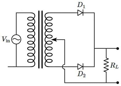 (a) D1 and D2 both are forward biased
(b) D1 and D2 both are reverse biased
(c) D1 is forward biased, D2 is reverse biased
(d) D1 is reverse biased, D2 is forward biased
Ans: (d)
Vin = 220 × sin(100πt) volt
Given: t = 15 ms = 0.015 s
ω = 100π
2π / T = 100π
⇒ T = 1 / 50 s
⇒ T = 0.02 s
Now, t = (3T / 4)
i.e., the signal is in the negative half cycle.
So now the negative half cycle is fed to the circuit, making D1 reverse biased and D2 forward biased.
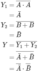
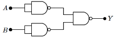
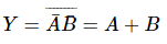
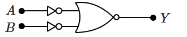
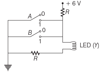
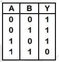
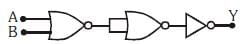
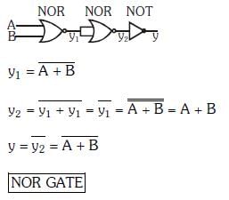
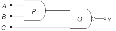
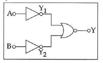
Q2: The output Y of the given logic implementation is similar to the output of which gate? (NEET 2025)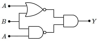 (a) OR
(b) NOR
(c) AND
(d) NAND
Ans: (b)
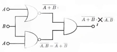
Thus the output Y will be

The correct option is b) NOR gate.
2024
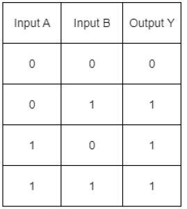
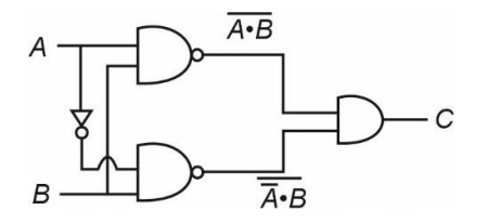
Q1: A logic circuit provides the output Y as per the following truth table: (NEET 2024)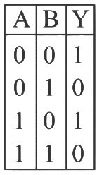 The expression of the output Y is :
(a) 
(b) 
(c) 
(d) B
Ans: (c) According to given truth table, output is independent on value of A
∴ Output 
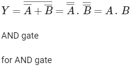
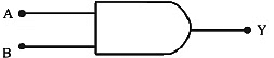
Q2: The output ( Y ) of the given logic gate is similar to the output of an/a (NEET 2024)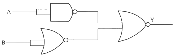 (a) NAND gate
(b) NOR gate
(c) OR gate
(d) AND gate
Ans: (d)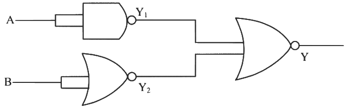
= A.B is similar to output of AND gate.
Q3: Consider the following statements A and B and identify the correct answer : (NEET 2024)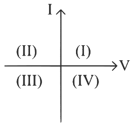 A. For a solar-cell, the I-V characteristics lies in the IV quadrant of the given graph.
B. In a reverse biased p n junction diode, the current measured in (μA), is due to majority charge carriers.
(a) A is correct but B is incorrect
(b) A is incorrect but B is correct
(c) Both A and B are correct
(d) Both A and B are incorrect
Ans: (a)
A : Solar cell characteristics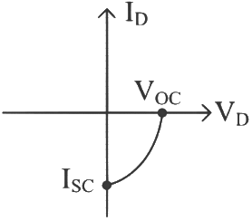 B : In reverse biased pn junction diode, the current measured in (μA), is due to minority charge carrier.
Q4: Choose the correct circuit which can achieve the bridge balance : (NEET 2024)
(a) 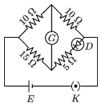
(b) 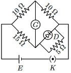
(c) 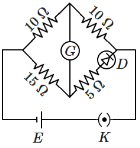
(d) 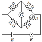
Ans: (d)
To Balance Bridge P/Q = R/S
Here P = 10 Ω
Q = 10 Ω
R = 15 Ω
and S = 5 + Rdiode
where Rdiode should be 10 Ω to Balance bridge.
Q5: A solar cell is a: (NEET 2024)
(a) forward biased Zener diode.
(b) type of light-emitting diode.
(c) diode working on the principle of photo-voltaic effect.
(d) type of photo-diode with external biasing.
Ans: (c)
A solar cell works on the principle of the photo-voltaic effect, where light energy (photons) is absorbed by a semiconductor material, generating electron-hole pairs, which then create a voltage (and current) that can be used as electrical power.
Let's analyze the options:
(a) Forward biased Zener diode: This is incorrect. A Zener diode is used in reverse bias to maintain a constant voltage, and a solar cell works based on the photo-voltaic effect, not on Zener breakdown.
(b) Type of light-emitting diode: This is incorrect. A light-emitting diode (LED) emits light when current passes through it, whereas a solar cell generates electricity from light.
(c) Diode working on the principle of photo-voltaic effect: This is correct. A solar cell is a photo-diode that works based on the photo-voltaic effect, converting light energy into electrical energy.
(d) Type of photo-diode with external biasing: This is incorrect. A solar cell is a photo-diode, but it works without external biasing, relying on the photo-voltaic effect to generate current.
Correct Answer: (c) Diode working on the principle of photo-voltaic effect.
Q6: Which input (A,B)−output (Y) combination correctly represents the given logic circuit? (NEET 2024)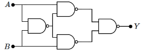 (a) A = 1, B = 1, Y = 1
(b) A = 0, B = 1, Y = 1
(c) A = 1, B = 0, Y = 0
(d) A = 0, B = 0, Y = 1
Ans: (b)
Circuit Description:
The circuit has two inputs: A and B, and the output is Y.
The circuit contains AND gates and a NAND gate.
Analysis:
First AND Gate: The first logic gate takes A and B as inputs. The output of the AND gate will be: A AND B.
Second AND Gate: The second AND gate has the output from the first AND gate and A as inputs. The output of this gate will be: (A AND B) AND A which simplifies to A AND B.
NAND Gate: The final output is taken from a NAND gate. The NAND gate takes the outputs of the second AND gate and input B. The output will be: NOT (A AND B).
Input-Output Combination:
When A = 1 and B = 1: The output of the AND gates is 1, and the output of the NAND gate is: NOT (1 AND 1) = 0.
When A = 0 and B = 1: The output of the AND gates is 0, and the output of the NAND gate is: NOT (0) = 1.
When A = 1 and B = 0: The output of the AND gates is 0, and the output of the NAND gate is: NOT (0) = 1.
When A = 0 and B = 0: The output of the AND gates is 0, and the output of the NAND gate is: NOT (0) = 1.
Correct Answer: The correct input-output combination that satisfies the circuit is A = 0, B = 1, Y = 1.
Correct Option: (b) A = 0, B = 1, Y = 1.
Q7: Zener diode works: (NEET 2024)
(a) in forward bias only.
(b) in reverse bias only.
(c) as a voltage regulator in forward bias and as a simple pn junction diode in reverse bias.
(d) as a voltage regulator in reverse bias and as a simple pn junction diode in forward bias.
Ans: (d)
A Zener diode is designed to operate primarily in reverse bias. It is used as a voltage regulator because it maintains a constant voltage across it when the reverse voltage exceeds a specific Zener breakdown voltage.
- In forward bias, the Zener diode behaves like a regular PN junction diode, allowing current to pass through once the threshold voltage is exceeded.
- In reverse bias, when the reverse voltage exceeds the Zener breakdown voltage, the Zener diode allows current to flow, but it maintains a constant voltage (the Zener voltage) across it, making it useful as a voltage regulator.
Correct Answer: (d) as a voltage regulator in reverse bias and as a simple pn junction diode in forward bias.
Q8: The I-V characteristics shown below are exhibited by a: (NEET 2024)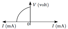 (a) Light-emitting diode
(b) Zener diode
(c) Photodiode
(d) Solar cell
Ans: (d)
The given I-V characteristic curve shows a device that produces current when exposed to light (positive current for positive voltage). This characteristic is shown by a solar cell. Solar cells convert light energy into electrical energy. The other options have different I-V characteristics.
The I-V characteristics of solar cell is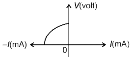
Q9: When the output of an OR gate is applied as input to a NOT gate, then the combination acts as a: (NEET 2024)
(a) NAND gate
(b) NOR gate
(c) AND gate
(d) OR gate
Ans: (b)
When the output of an OR gate is applied as input to a NOT gate, the combination acts as a NOR gate.
Here's why:
An OR gate produces a high output (1) when at least one of the inputs is 1. The truth table of an OR gate is:
- 0 OR 0 = 0
- 0 OR 1 = 1
- 1 OR 0 = 1
- 1 OR 1 = 1
A NOT gate inverts the input. So, when the output of the OR gate is passed through a NOT gate, it inverts the logic, which results in the behavior of a NOR gate. The truth table for a NOR gate is:
- NOT (0 OR 0) = 1
- NOT (0 OR 1) = 0
- NOT (1 OR 0) = 0
- NOT (1 OR 1) = 0
Thus, the combination of an OR gate followed by a NOT gate results in a NOR gate.
Correct Answer: (b) NOR gate.
Q10: The output Y for the inputs A and B of the given logic circuit is: (NEET 2024)
 (a) A . B
(b) 
(c) A + B
(d) 
Ans: (c)
The circuit consists of two OR gates whose outputs are then applied as inputs to another OR gate. Therefore, the logic expression for the output Y is:
Y = (A + B)
2023
Q1: On the basis of electrical conductivity, which one of the following material has the smallest resistivity? (NEET 2023)
(a) Germanium
(b) Silver
(c) Glass
(d) Silicon
Ans: (b)
Electrical conductivity is a measure of a material's ability to conduct an electric current. The higher the conductivity, the lower the resistivity. So, if we are looking for the material with the smallest resistivity, we are looking for the material with the highest electrical conductivity.
Among the options given, silver (Option B) is known to have the highest electrical conductivity and thus, the smallest resistivity. Germanium (Option A) and silicon (Option D) are semiconductors, meaning they have moderate conductivity that can be manipulated, while glass (Option C) is generally a poor conductor, or an insulator. Therefore, silver is the correct answer.
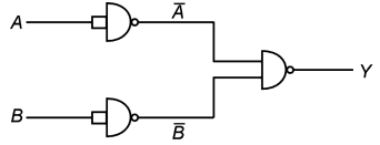
Q2: The given circuit is equivalent to:
 (a)
(a) 
(b) 
(c) 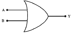
(d) 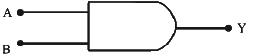
Ans: (d)
Q3: A p-type extrinsic semiconductor is obtained when Germanium is doped with: (NEET 2023)
(a) Antimony
(b) Phosphorous
(c) Arsenic
(d) Boron
Ans: (d)
For p type semiconductor trivalent impurity added
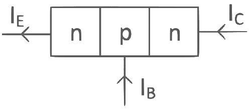
Q4: The below figure shows the circuit symbol of a transistor. Select the correct statements given below:
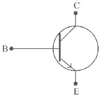
(A) The transistor has two segments of p-type semiconductor separated by a segment of n-type semiconductor. (NEET 2023)
(B) The emitter is of moderate size and heavily doped.
(C) The central segment is thin and lightly doped.
(D) The emitter base junction is reverse biased in common emitter amplifier circuit.
(a) (C) and (D)
(b) (A) and (D)
(c) (A) and (B)
(d) (B) and (C)
Ans: (d)
In given symbol, emitter current leave from emitter so transistor is NPN
for active mode emitter base junction is forward bias and base-collector junction is reverse bias.
Q5: Given below are two statements: (NEET 2023)
Statement I: Photovoltaic devices can convert optical radiation into electricity.
Statement II: The Zener diode is designed to operate under reverse bias in the breakdown region.
In the light of the above statements, choose the most appropriate answer from the options given below.
(a) Both Statement I and Statement II are correct
(b) Both Statement I and Statement II are incorrect
(c) Statement I is correct but Statement II is incorrect
(d) Statement I is incorrect but Statement II is correct
Ans: (a)
Solution: Both Statements are correct.
I: Photovoltaic devices convert optical radiation into electricity.
II: The Zener diode is designed to operate under reverse bias in the breakdown region. e.g., Zener diode as a voltage regulator.
Q6: A full wave rectifier circuit consists of two p-n junction diodes, a center-tapped transformer, a capacitor, and a load resistance. Which of these components removes the ac ripple from the rectified output? (NEET 2023)
(a) A centre-tapped transformer
(b) p-n junction diodes
(c) Capacitor
(d) Load resistance
Ans: (c)
Solution: The capacitor removes the AC ripple from the rectified output.
Q7: For the following logic circuit, the truth table is (NEET 2023)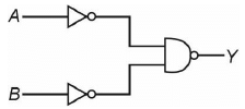 (a)
(a)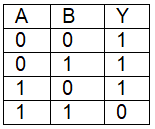
(b)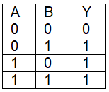
(c)
(d)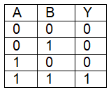
Ans: (b)
Solution: 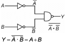
It is OR gate.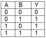
2022
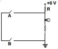
Q1: Identify the equivalent logic gate represented by the given circuit
(a) NAND
(b) OR
(c) NOR
(d) AND
Ans: (b)
The given circuit clearly indicates that the bulb will glow when either of the switches are closed.
The corresponding truth table will be
This suggests that it will correspond to OR gate.
Q2: The incorrect statement about the property of a Zener diode is :
(a) p and n regions of Zener diode are heavily doped
(b) Zener voltage remains constant at breakdown
(c) It is designed to operate under reverse bias
(d) Depletion region formed is very wide
Ans: (d)
Zener diode is special purpose p-n junction diode, which is generally operated in reverse bias for its operation of voltage regulation. It is a heavily doped p-n junction. Due to large doping concentration depletion width is narrower.
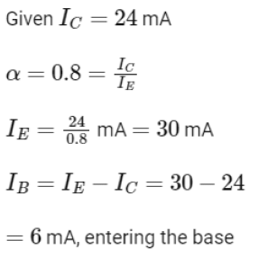
Q3: The collector current in a common base amplifier using n-p-n transistor is 24 mA. If 80% of the electrons released by the emitter is accepted by the collector, then the base current is numerically :
(a) 3 mA and entering the base
(b) 6 mA and leaving the base
(c) 3 mA and leaving the base
(d) 6 mA and entering the base
Ans: (d)
Q4: In the given circuits (a), (b) and (c), the potential drop across the two p-n junctions are equal in
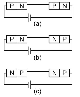
(a) Circuit (a) only
(b) Circuit (b) only
(c) Circuit (c) only
(d) Both circuits (a) and (c)
Ans: (d)
Potential drops across the p-n junctions will be same if either both junctions are forward biased or both junction are reverse biased.
In figure (a) and (c), both junctions are forward biased therefore both have same potential.
In figure (b) first junction is forward biased and second junction is reverse biased, so both junctions have different potential difference.
Q5: As the temperature increases, the electrical resistance
(a) Increases for both conductors and semiconductors
(b) Decreases for both conductors and semiconductors
(c) Increases for conductors but decreases for semiconductors
(d) Decreases for conductors but increases for semiconductors
Ans: (c)
As the temperature increases the resistivity of the conductor increases hence the electrical resistance increases. However for semiconductor the resistivity decreases with the temperature. Hence electrical resistance of semiconductor decreases.
Q6: In the given circuits (a), (b) and (c), the potential drop across the two p-n junctions are equal in:
 (a) Both circuits (a) and (c)
(b) Circuit (a) only
(c) Circuit (b) only
(d) Circuit (c) only
Ans: (a)
Solution:
Potential drops across the p-n junctions will be the same if either both junctions are forward biased or both junctions are reverse biased.
In figures (a) and (c), both junctions are forward-biased therefore both have the same potential.
In Figure (b) the first junction is forward biased and the second junction is reverse biased, so both junctions have different potential differences.
Q7: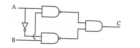 The truth table for the given logic circuit is
(a)
(b)
(c)
(d)
Ans: (b)
Solution: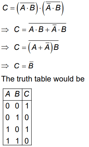
Q9: In half wave rectification, if the input frequency is 60 Hz, then the output frequency would be
(a) 30 Hz
(b) 60 Hz
(c) 120 Hz
(d) Zero
Ans: (b)
Solution: In half-wave rectifier, the output frequency is the same as that of the input frequency.
2021
Q1: The electron concentration in an n-type semiconductor is the same as the hole concentration in a p-type semiconductor. An external field (electric) is applied across each of them. Compare the currents in them.
(a) Current in n-type > current in p-type.
(b) No current will flow in p-type, current will only flow in n-type.
(c) Current in n-type = current in p-type.
(d) Current in p-type > current in n-type.
Ans: (a)
Solution: In N-type semiconductors majority charge carriers are e- an P-type semiconductors majority charge carriers are holes.
I = neAVd = neA(μE)
μe > μh
⇒ Ie > Ih
Q2: Consider the following statements (A) and (B) and identify the correct answer.
A. A zener diode is connected in reverse bias when used as a voltage regulator.
B. The potential barrier of the p-n junction lies between 0.2 V to 0.3 V.
(a) (A) is correct and (B) is incorrect.
(b) (A) is incorrect and (B) is correct.
(c) (A) and (B) both are correct.
(d) (A) and (B) both are incorrect.
Ans: (a)
Solution: (A) is correct and (B) is incorrect.
Q3: For the given circuit, the input digital signals are applied at the terminals A, B, and C. What would be the output at the terminal y? 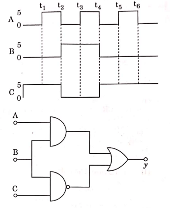
(a)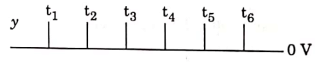
(b) 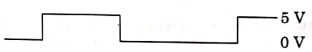
(c)
(d) 
Ans: (c)
Solution:
(i) 0 to t1 A = 0, B = 0, C = 1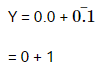
= 1
(ii) t1 to t2 A = 1, B = 0, C = 1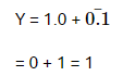
(iii) t2 to t3 A = 0, B = 1, C = 0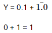
2020
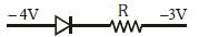
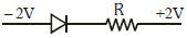
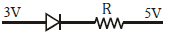
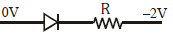
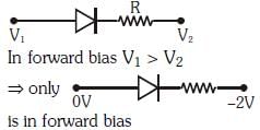
Q1: Out of the following which one is a forward biased diode?
Ans: (d)
A p-n junction diode is in forward biased when p-side is connected with more positive potential than n-side.
Since, 0V > − 3V.
Hence in option (d), diode circuit is in forward biased.
Q2: An intrinsic semiconductor is converted into n-type extrinsic semiconductor by doping it with
(a) phosphorous
(b) aluminium
(c) silver
(d) germanium
Ans: (a)
When a pentavalent (phosphorous) impurities is doped with intrinsic semiconductor (Ge, Si), then n-type semiconductor is formed.
Q3: The solids which have the negative temperature coefficient of resistance are
(a) insulator only
(b) semiconductors only
(c) insulators and semiconductors
(d) metals
Ans: (c)
Insulators and semiconductors are those solids, which have negative temperature coefficient of resistance.
As, when temperature increases number of free electrons increases in both insulator and semiconductor.
Hence, correct option is (c).
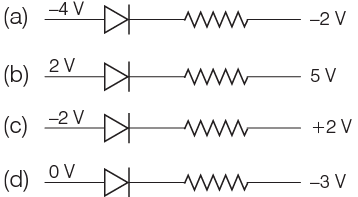
Q4: A n-p-n transistor is connected in common emitter configuration (see figure) in which collector voltage drop across load resistance (800Ω) connected to the collector circuit is 0.8 V. The collector current is
(a) 2 mA
(b) 0.1 mA
(c) 1 mA
(d) 0.2 mA
Ans: (c)
According to given circuit diagram.
RC = 800 Ω
Vcc = 8V

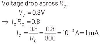
Q5: Which of the following gate is called universal gate?
(a) OR gate
(b) AND gate
(c) NAND gate
(d) NOT gate
Ans: (c)
NAND and NOR gate are called universal gate because all type of logic gates and Boolean expressions can be realised with the help of NAND and NOR gate.
Q6: For transistor action, which of the following statements is correct?
(a) Both the emitter junction as well as the collector junction are forward-biased.
(b) The base region must be very thin and lightly doped.
(c) Base, emitter, and collector regions should have the same doping concentrations.
(d) Base, emitter, and collector regions should have the same size.
Ans: (b)
Solution:
For a transistor action, the base junction must be lightly doped so that the base region is very thin.
Q7: For the logic circuit shown, the truth table is : 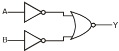
(a)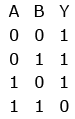
(b)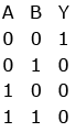
(c)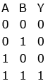
(d)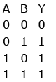
Ans: (c)
Solution: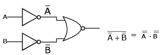
= A.B (using de-Morgan’s rule)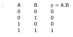
Q8: The increase in the width of the depletion region in a p-n junction diode is due to:
(a) Both forward bias and reverse bias
(b) increase in forward current
(c) forward bias only
(d) reverse bias only
Ans: (d)
Solution:
The increase in the width of the depletion region in a p-n junction diode is due to reverse bias only.
2019
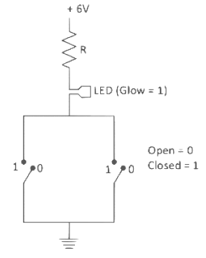
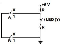
Q1: The circuit diagram shown here corresponds to the logic gate,
(a) NOR
(b) AND
(c) OR
(d) NAND
Ans: (a)
From the circuit diagram given below, it can be seen that the current will flow to ground if any of the switch is closed.
Also, the LED will only glow when current flows through it.
Q2: An LED is constructed from a p-n junction diode using GaAsP. The energy gap is 1.9 eV. The wavelength of the light emitted will be equal to
(a) 10.4 ×10⁻²⁶ m
(b) 654 nm
(c) 654 Å
(d) 654 ×10−11 m
Ans: (b)
The energy of light of wavelength λ is given by
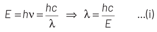
Here, h = Planck’s constant = 6.63 × 10 −34 J-s
c = speed of light = 3 × 10 8 m/s
E = energy gap = 1.9 eV = 1.9 × 1.6 × 10 −19 J
Substituting the given values in Eq. (i), we get
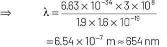
Thus, the wavelength of light emitted from LED will be 654 nm.
Q3: The correct Boolean operation represented by the circuit diagram drawn is:
(a) AND
(b) OR
(c) NAND
(d) NOR
Ans: (c)
Solution:
From the given logic circuit LED will glow, when the voltage across LED is high.
Truth Table
This is output of the NAND gate.
Q4: For a p-type semiconductor, which of the following statements is true?
(a) Electrons are the majority carriers and trivalent atoms are the dopants.
(b) Holes are the majority carriers and trivalent atoms are the dopants.
(c) Holes are the majority carriers and pentavalent atoms are the dopants.
(d) Electrons are the majority carriers and pentavalent atoms are the dopants.
Ans: (b)
Solution:
In a p-type semiconductor, an intrinsic semiconductor is doped with trivalent impurities, that create deficiencies of valence electrons called holes which are majority charge carriers.
2018
Q1: In the circuit shown in the figure, the input voltage Vi is 20 V, VBE = 0 and VCE = 0. The values of IB , IC and β are given by
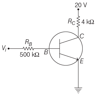
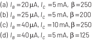
Ans: (d)
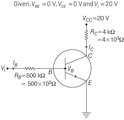
Applying Kirchhoff’s law to the base-emitter loop, we get
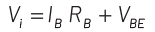
Substituting the values, we get
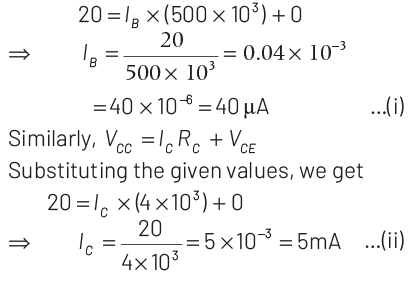
Current gain is given as
Q2: In the combination of the following gates the output Y can be written in terms of inputs A and B as: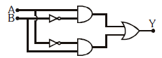
(a)
(b)
(c)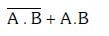
(d)
Ans: (b)
Solution:
Q3: In a p-n junction diode, change in temperature due to heating:
(a) affects only reverse resistance
(b) affects only forward resistance
(c) does not affect the resistance of the p-n junction
(d) affects the overall V - I characteristics of p-n junction
Ans: (d)
Solution:
Affects the overall V - I characteristic of the p-n junction.
On heating, the number of electron-hole pairs increases, so the overall resistance of the diode will change.
Hence, forward biasing and reversed biasing both are changed.
2017
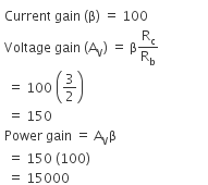
Q1: In a common emitter transistor amplifier, the audio signal voltage across the collector is 3V. The resistance of the collector is 3 kΩ. If the current gain is 100 and the base resistance is 2 kΩ, the voltage and power gain of the amplifier is:
(a) 15 and 200
(b) 150 and 15000
(c) 20 and 2000
(d) 200 and 1000
Ans: (b)
Solution:
Q2: The given electrical network is equivalent to:
(a) OR gate
(b) NOR gate
(c) NOT gate
(d) AND gate
Ans: (b)
Solution:
Q3: Which one of the following represents a forward bias diode?
(a)
(b)
(c)
(d)
Ans: (d)
Solution:
2016
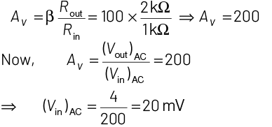
Q1: For CE transistor amplifier, the audio signal voltage across the collector resistance of 2 kΩ is 4 V. If the current amplification factor of the transistor is 100 and the base resistance is l kΩ, then the input signal voltage is
(a) 10 mV
(b) 20 mV
(c) 30 mV
(d) 15 mV
Ans: (b)
Voltage amplification is
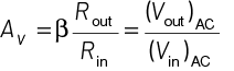
Given, collector resistance = Rout = 2kΩ
Current amplification factor, β = 100
Base resistance, Rin = 1 kΩ
Output signal voltage = 4 V
Putting all the values in given equation, we get
Q2: What is the output Y in the following circuit, when all the three inputs A, B, C are first 0 and then 1?
(a) 0, 1
(b) 0, 0
(c) 1, 0
(d) 1, 1
Ans: (c)
Output of the given circuit is given by
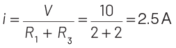
Q3: The given circuit has two ideal diodes connected as shown in the figure below. The current flowing through the resistance R1 will be
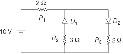
(a) 2.5 A
(b) 10.0 A
(c) 1.43 A
(d) 3.13 A
Ans: (a)
We know that a diode only conducts in forward biased condition. In the given circuit, the diode D1 will be in reverse bias, so it will block the current and diode D2 will be in forward bias, so it will pass the current
Q4: To get output 1 for the following circuit, the correct choice for the input is : 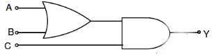
(a) A = 1, B = 0, C = 1
(b) A = 0, B =1, C = 0
(c) A = 1, B = 0, C = 0
(d) A = 1, B = 1, C = 0
Ans: (a)
Solution:
The resultant boolean expression of the above logic circuit is given by,
Y = (A+B).C
Using the inputs given in the options,
If A = 0, B = 0,C = 0, we have
Y = (0+0).0
i.e., Y = 0
If A = 1, B = 1, C = 0, then we have
Y = (1+1).0
i.e., Y = 1.0 = 0
If A = 1, B = 0, C = 1, then
Y = (1+0).1
i.e., Y = 1.1 = 1
If A = 0, B = 1, C = 0, then
Y = (0+1).0
i.e., Y = 1.0
Y = 0
Therefore, output Y = 1 only when inputs A = 1, B = 0 and C = 1.
Q5: Consider the junction diode as ideal. The value of current flowing through AB is :
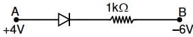
(a) 10-3 A
(b) 0 A
(c) 10-2 A
(d) 10-1 A
Ans: (c)
Solution:
For diode as ideal
I = ΔV/R = 4-(-6)/ 103 = 10-2 A
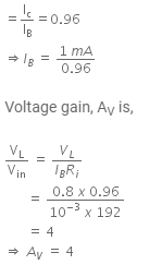
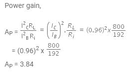
Q6: An NPN transistor is connected in a common emitter configuration in a given amplifier. A load resistance of 800 Ω is connected in the collector circuit and the voltage drop across it is 0.8 V. If the current amplification factor is 0.96 and the input resistance of the circuit is 192Ω, the voltage gain and the power gain of the amplifier will respectively be :
(a) 4, 3.69
(b) 4, 3.84
(c) 3.69, 3.84
(d) 4, 4
Ans: (b)
Solution:
Given,
Resistance across the load, RL = 800 ohm
The voltage drop across the load, VL = 0.8 V
The input resistance of the circuit, Ri = 192 ohm
The collector current is given by,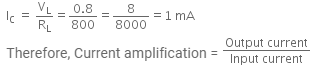
2015
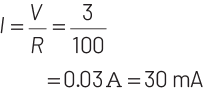
Q1: In the given figure, a diode D is connected to an external resistance R = 100 Ω and an e.m.f of 3.5 V. If the barrier potential developed across the diode is 0.5 V, the current in the circuit will be
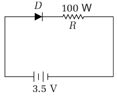
(a) 30 mA
(b) 40 mA
(c) 20 mA
(d) 35 mA
Ans: (a)
Given, external resistance R = 100 Ω and an emf is 3.5 V.
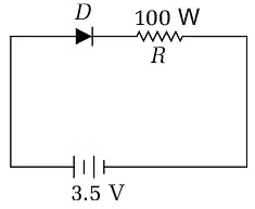
Potential barrier across the diode is 0.5 V,
Potential difference on
R = 3.5 V − 0.5 V = 3.0 V
Current in circuit,
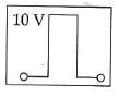
Q2: If in a p-n junction, a square input signal of 10 V is applied, as shown,
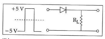
then the output across RL will be :
(a)
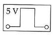
(b)
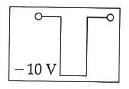
(c)
(d)
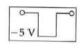
Ans: (a)
Solution:
As it is forward biased it takes positive value. Hence, option (A) is correct.
(a) NOR
(b) OR
(c) NAND
(d) AND
Ans: (d)
Solution: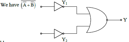
Truth table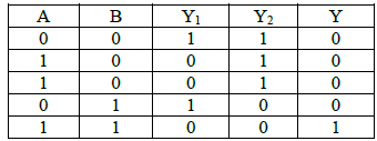
This corresponds to AND gate
2014
Q1: The given graph represents the V−I characteristics of a semiconductor device.
Which of the following statements is correct?
(a) It is for a photodiode and points A and B represent open circuit voltage and current,
respectively
(b) It is for an LED and points A and B represent open circuit voltage and short circuit current, respectively
(c) It is a V−I characteristic for solar cells where, point A represents open circuit voltage and
point B short circuit current
(d) It is for a solar cell and points A and B represent open circuit voltage and current,
respectively
Ans: (c)
Q2: The barrier potential of a p-n junction depends on:
(a) type of semiconductor material
(b) amount of doping
(c) temperature
Which one of the following is correct?
(a) (b) and (c) only
(b) (a),(b) and (c)
(c) (a) and (b) only
(d) (b) only
Ans: (b)
Solution:
Barrier potential depends on the material used to make the p-n junction diode (whether it is Si or Ge).
It should also depend on the amount of doping due to which the number of majority charge carriers will change. Also, it depends on temperature due to which the number of minority carriers will change.
|
74 videos|314 docs|88 tests
|
FAQs on NEET Previous Year Questions (2014-2025): Semiconductor Electronics - Physics Class 12
| 1. What are semiconductors and why are they important in electronics? |  |
| 2. What is the difference between intrinsic and extrinsic semiconductors? | |
| 3. How do diodes function in semiconductor electronics? | |
| 4. What role do transistors play in semiconductor devices? | |
| 5. What are some common applications of semiconductor electronics in daily life? | |


MCQs
,Viva Questions
,Sample Paper
,Previous Year Questions with Solutions
,Objective type Questions
,Free
,Extra Questions
,mock tests for examination
,NEET Previous Year Questions (2014-2025): Semiconductor Electronics | Physics Class 12
,practice quizzes
,ppt
,Important questions
,study material
,Exam
,NEET Previous Year Questions (2014-2025): Semiconductor Electronics | Physics Class 12
,Summary
,video lectures
,Semester Notes
,shortcuts and tricks
,NEET Previous Year Questions (2014-2025): Semiconductor Electronics | Physics Class 12
,past year papers
;


NEET Previous Year Questions (2014-2025): Semiconductor Electronics Free PDF Download
Importance of NEET Previous Year Questions (2014-2025): Semiconductor Electronics
NEET Previous Year Questions (2014-2025): Semiconductor Electronics Notes
NEET Previous Year Questions (2014-2025): Semiconductor Electronics NEET
Study NEET Previous Year Questions (2014-2025): Semiconductor Electronics on the App
|
© EduRev
|
Education Revolution
|


|


