Q1: If the following switching devices have similar power ratings, which one of them is the fastest? (2024)
(a) SCR
(b) GTO
(c) IGBT
(d) Power MOSFET
Ans: (d)
Q2: A semiconductor switch needs to block voltage V of only one polarity (V > 0) during OFF state as shown in figure (i) and carry current in both directions during ON state as shown in figure (ii). Which of the following switch combination(s) will realize the same? (2023)
 (a)
(a)  (b)
(b)  (c)
(c)  (d)
(d) 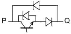 Ans: (a, d)
Sol: I-V characteristic of given switch :
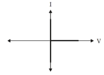 this characteristic shows by options (A) and (D) switch.
Q3: A charger supplies 100 W at 20 V for charging the battery of a laptop. The power devices, used in the converter inside the charger, operate at a switching frequency of 200 kHz. Which power device is best suited for this purpose? (2022)
(a) IGBT
(b) Thyristor
(c) MOSFET
(d) BJT
Ans: (c)
Sol: Ratings of different power devices:
BJT : 1200 V, 800 A, (10 - 20)kHz
SCR : 10000 V, 3000 A
IGBT : 1200 V, 500 A, 50 kHz
MOSFET : 500 V, 140 A, 1 MHz
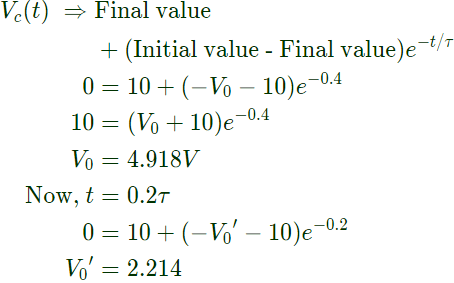
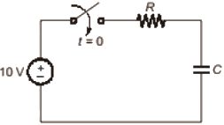
Q4: A resistor and a capacitor are connected in series to a 10 V dc supply through a switch. The switch is closed at t = 0, and the capacitor voltage is found to cross 0 V at t = 0.4τ, where τ is the circuit time constant. The absolute value of percentage change required in the initial capacitor voltage if the zero crossing has to happen at t = 0.2τ is _______ (rounded off to 2 decimal places). (2020)
(a) 24.24
(b) 78.83
(c) 12.45
(d) 54.99
Ans: (d)
Sol: If initial charge polarities on the capacitor is opposite to the supply voltage then only the capacitor voltage crosses the zero line.

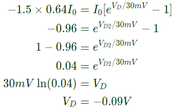
Q5: A non-ideal diode is biased with a voltage of -0.03 V, and a diode current of I1 is measured. The thermal voltage is 26 mV and the ideality factor for the diode is 15/13. The voltage, in V, at which the measured current increases to 1.5 I1 is closest to: (2020)
(a) -0.02
(b) -0.09
(c) -1.5
(d) -4.5
Ans: (b)
Sol: 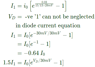
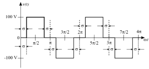
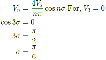
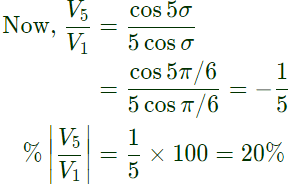
Q6: A single-phase inverter is fed from a 100 V dc source and is controlled using a quasisquare wave modulation scheme to produce an output waveform, v(t). as shown. The angle σ is adjusted to entirely eliminate the 3rd harmonic component from the output voltage. Under this condition, for v(t), the magnitude of the 5th harmonic component as a percentage of the magnitude of the fundamental component is _______(rounded off to 2 decimal places). (2020)
(a) 15
(b) 10
(c) 20
(d) 25
Ans: (c)
Sol: Using result,
Q7: Four power semiconductor devices are shown in the figure along with their relevant terminals. The device(s) that can carry dc current continuously in the direction shown when gated appropriately is (are) (2018)
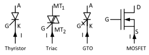 (a) Triac only
(b) Triac and MOSFET
(c) Triac and GTO
(d) Thyristor and Triac
Ans: (b)
Q8: For the power semiconductor devices IGBT, MOSFET, Diode and Thyristor, which one of the following statements is TRUE? (SET-1 (2017))
(a) All of the four are majority carrier devices.
(b) All the four are minority carrier devices
(c) IGBT and MOSFET are majority carrier devices, whereas Diode and Thyristor are minority carrier devices.
(d) MOSFET is majority carrier device, whereas IGBT, Diode, Thyristor are minority carrier devices.
Ans: (d)
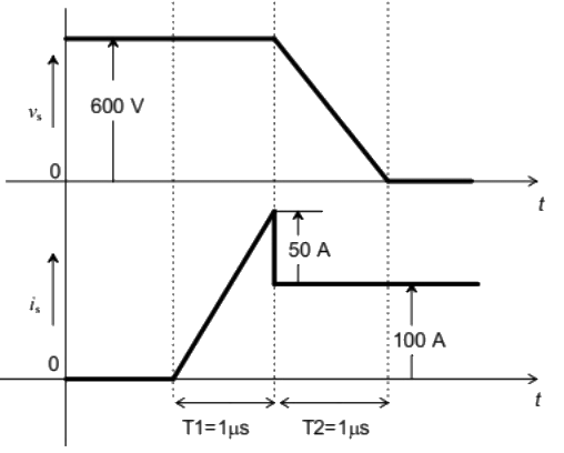
Q9: The voltage (vs) across and the current (is) through a semiconductor switch during a turn-ON transition are shown in figure. The energy dissipated during the turn-ON transition, in mJ, is _______. (SET-1 (2016))
 (a) 25
(b) 50
(c) 75
(d) 100
Ans: (c)
Sol: 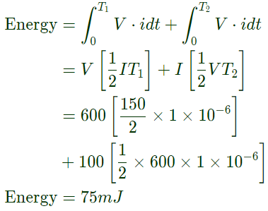
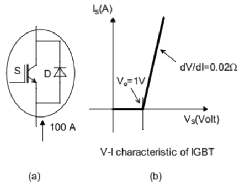
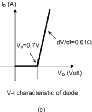
Q10: A steady dc current of 100 A is flowing through a power module (S,D) as shown in Figure (a). The V-I characteristics of the IGBT (S) and the diode (D) are shown in Figures (b) and (c), respectively. The conduction power loss in the power module (S,D), in watts, is ________. (SET-1 (2016))
 (a) 100
(b) 135
(c) 240
(d) 170
Ans: (d)
Sol: No current flows through IGBT. So current flows only in diode. Equivalent circuit of diode is as shown below,

 Power loss during conduction,
P = V x I
= 1.7 x 100 = 170 W
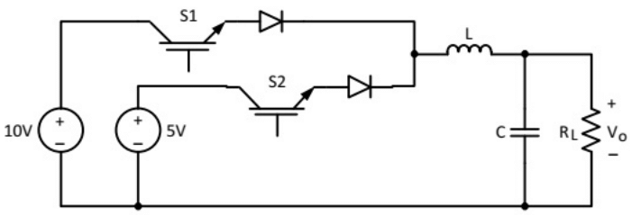
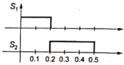
Q11: The circuit shown is meant to supply a resistive load RL from two separate DC voltage sources. The switches S1 and S2 are controlled so that only one of them is ON at any instant. S1 is turned on for 0.2 ms and S2 is turned on for 0.3 ms in a 0.5 ms switching cycle time period. Assuming continuous conduction of the inductor current and negligible ripple on the capacitor voltage, the output voltage V0 (in Volt) across RL is ___________. (SET-1 (2015))
 (a) 3
(a) 3
(b) 7
(c) 9
(d) 11
Ans: (b)
Sol: 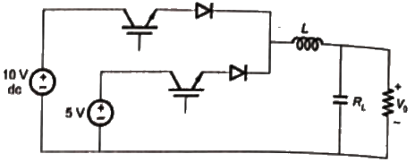 S1 is turn ON for 0.2 ms
S2 is turn ON for 0.3 ms.
Switching cycle time period is 0.5 ms.
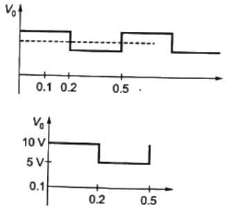
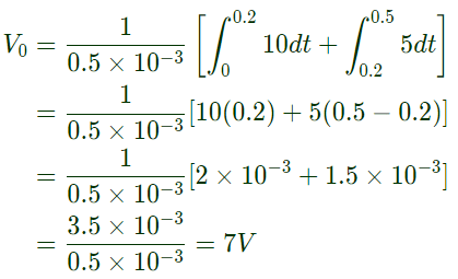
 the output voltage V0 across RL is
Q12: Figure shows four electronic switches (i), (ii), (iii) and (iv). Which of the switches can block voltages of either polarity (applied between terminals 'a' and 'b') when the active device is in the OFF state? (SET-1 (2014))
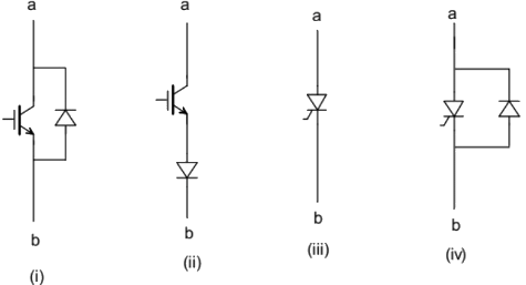 (a) (i), (ii) and (iii)
(b) (ii), (iii) and (iv)
(c) (ii) and (iii)
(d) (i) and (iv)
Ans: (c)
Sol: 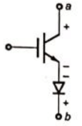 As given that the active device is in OFF state it means the device can block the voltage when 'a' is positive with respect to 'b' and when 'b' is positive with respect to 'a' then the diode is reverse baised and voltage is blocked.
 When 'a' is positive with respect to 'b', as given the device is OFF so it will block the voltage.
When 'b' is positive with respect to 'a' it will block the voltage.
Where as the other two devices will conduct when 'b' is positive with respect to 'a'.
Q13: The typical ratio of latching current to holding current in a 20 A thyristor is (2012)
(a) 5
(b) 2
(c) 1
(d) 0.5
Ans: (b)
Sol: For medium power thyristor of rating 6 A to 60 A the ratio of the latching current to holding current is 1.5 to 2.
Q14: A voltage commutated chopper circuit, operated at 500 Hz, is shown below.
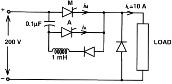 If the maximum value of load current is 10 A, then the maximum current through the main (M) and auxiliary (A) thyristors will be (2011)
(a) iMmax = 12A and iAmax =10A
(b) iMmax = 12A and iAmax = 2A
(c) iMmax = 10A and iAmax = 12A
(d) iMmax = 10A and iAmax = 8A
Ans: (a)
Sol: When main thyristor (M) is turned on, an oscillatory current in the circuit C, M, L and diode is set up and it is given by 
Peak value of current through capacitor
 Current through main thyristor
 So maximum value of
When auxiliary thyristor (A) is turned on, capacitor voltage applies a reverse voltage across main thyristor and main thyristor is turned off. The load current is now carried by C nad auxiliary thyristor . Current through auxiliary thyristor,
iA = I0
maximum value of iA = maximum value of I0 = 10A.
Q15: Circuit turn-off time of an SCR is defined as the time (2011)
(a) taken by the SCR turn to be off
(b) required for the SCR current to become zero
(c) for which the SCR is reverse biased by the commutation circuit
(d) for which the SCR is reverse biased to reduce its current below the holding current
Ans: (c)
Sol: It is defined as the time between the instant anode current becomes zero and the instant reverse voltage is applied across SCR.
Q16: Figure shows a composite switch consisting of a power transistor (BJT) in series with a diode. Assuming that the transistor switch and the diode are ideal, the I-V characteristic of the composite switch is (2010)
 (a)
(a) (b)
(b)  (c)
(c) (d)
(d) 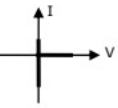 Ans: (c)
Sol: BJT blocks positive voltage and diode blocks negative voltage and both devices aloows positive current.
Q17: Match the switch arrangements on the top row to the steady-state V - I characteristics on the lower row. The steady state operating points are shown by large black dots. (2009)
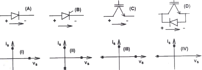 (a) A-I, B-II, C-III, D-IV
(b) A-II, B-IV, C-I, D-III
(c) A-IV, B-III, C-I, D-II
(d) A-IV, B-III, C-II, D-I
Ans: (c)
Sol: Device-A:
 When diode is forward baised (ON state), Vs = 0, is > 0
diode is reversed baised (OFF state) Vs < 0, is = 0:
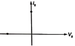
when thyristor is in reverse blocking mode, Vs < 0, is = 0
thyristor is in forward blocking, Vs > 0, is = 0
thyristor is in forward conduction mode, Vs = 0, is > 0
 When device is ON, Vs = 0, is > 0
The device is OFF, Vs > 0, is = 0
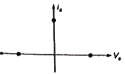 Reverse current can flow through the diode so is < 0 and Vs = 0
During ON state of the device Vs = 0, is > 0
During OFF state of the device, Vs = 0, is = 0

Q18: The circuit shows an ideal diode connected to a pure inductor and is connected to a purely sinusoidal 50 Hz voltage source. Under ideal conditions the current waveform through the inductor will look like. (2009)
 (a)
(a) 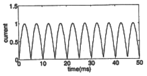 (b)
(b) 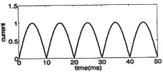 (c)
(c) 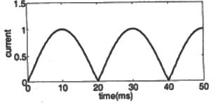 (d)
(d) 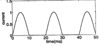 Ans: (c)
Sol: Frequency of the voltage source, f = 50Hz
Time period, 
During positive half cycle of the source voltage, 0 < t < T/2, energy is stored in the inductor and current increases.
During negative half cycle of the source voltage, T/2 ≤ t ≤ T, current decreases and energy stored in the inductor is delivered to source.
Q19: An SCR is considered to be a semi-controlled device because (2009)
(a) It can be turned OFF but not ON with a gate pulse.
(b) It conducts only during one half-cycle of an alternating current wave
(c) It can be turned ON but not OFF with a gate pulse.
(d) It can be turned ON only during one half-cycle of an alternating voltage
Ans: (c)
Sol: During one half cycle, SCR can be in forward blocking mode and by applying gate pulse, the SCR operates in forward conduction mode (ON state).
But SCR can not be turned OFF by applying gate pulse.
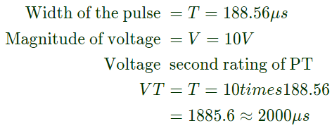
Q20: A 1:1 Pulse Transformer (PT) is used to trigger the SCR in the below figure. The SCR is rated at 1.5 kV, 250 A with IL = 250 mA, IH = 150 mA, and IGmax = 150 mA, IGmin = 100 mA. The SCR is connected to an inductive load, where L = 150 mH in series with a small resistance and the supply voltage is 200 V dc. The forward drops of all transistors/diodes and gate-cathode junction during ON state are 1.0 V
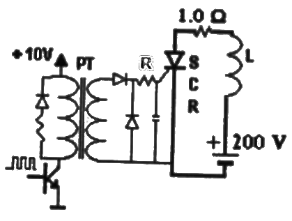 The minimum approximate volt-second rating of pulse transformer suitable for triggering the SCR should be : (volt-second rating is the maximum of product of the voltage and the width of the pulse that may applied) (2007)
(a) 2000 μV-s
(b) 200 μV-s
(c) 20 μV-s
(d) 2 μV-s
Ans: (a)
Sol: 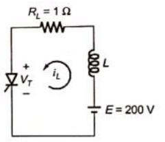 Forward voltage drop of SCR during ON-state
VT = 1V
 Gate pulse width required = time taken by i_a to rise up to
IL = T


 (a)
(a)  (b)
(b)  (c)
(c)  (d)
(d)  Ans: (a, d)
 this characteristic shows by options (A) and (D) switch.


 (a) Triac only
 (a) 25

 (a) 100
 Power loss during conduction,
 (a) 3
(a) 3 S1 is turn ON for 0.2 ms
 the output voltage V0 across RL is

 (a) (i), (ii) and (iii)
 As given that the active device is in OFF state it means the device can block the voltage when 'a' is positive with respect to 'b' and when 'b' is positive with respect to 'a' then the diode is reverse baised and voltage is blocked.
 When 'a' is positive with respect to 'b', as given the device is OFF so it will block the voltage.
 If the maximum value of load current is 10 A, then the maximum current through the main (M) and auxiliary (A) thyristors will be (2011)
 Current through main thyristor
 So maximum value of
 (a)
(a) (b)
(b)  (c)
(c) (d)
(d)  Ans: (c)
 (a) A-I, B-II, C-III, D-IV
 When diode is forward baised (ON state), Vs = 0, is > 0
 When device is ON, Vs = 0, is > 0
 Reverse current can flow through the diode so is < 0 and Vs = 0
 (a)
(a)  (b)
(b)  (c)
(c)  (d)
(d)  Ans: (c)
 The minimum approximate volt-second rating of pulse transformer suitable for triggering the SCR should be : (volt-second rating is the maximum of product of the voltage and the width of the pulse that may applied) (2007)
 Forward voltage drop of SCR during ON-state
 Gate pulse width required = time taken by i_a to rise up to
