Timers & Filters

The 555 Timer Circuit
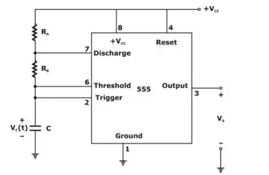
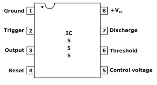 Pin diagram of 555 Timer
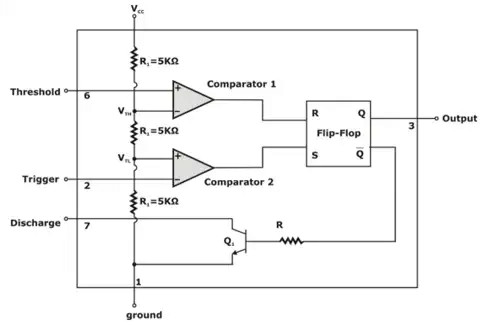 Block diagram representation of the internal circuit of the 555-IC timer
A block-diagram representation of the 555 timer is shown above. The internal circuit consists of two comparators, an SR flip-flop, a discharge transistor Q1 (used as a switch) and a resistive divider. A single supply VCC powers the device.
The resistive divider is formed by three equal resistors (each typically 5 kΩ) connected between VCC and ground. These establish the two reference voltages used by the comparators:
- Threshold voltage for comparator 1:VTH = (2/3) VCC
- Trigger voltage for comparator 2:VTL = (1/3) VCC
The SR flip-flop acts as a bistable device with complementary outputs Q and Q̄. When the flip-flop is in the set state, Q is high (≈ VCC) and Q̄ is low (≈ 0 V). In the reset state Q is low and Q̄ is high.

The comparators drive the flip-flop: the output of comparator 1 is connected to the reset input of the flip-flop and the output of comparator 2 to the set input. The external pins labelled Threshold and Trigger are connected respectively to the positive input of comparator 1 and the negative input of comparator 2. The collector of the discharge transistor Q1 is connected to the external Discharge pin. The flip-flop output Q is routed to the external Output pin of the IC.
Implementation of Monostable Multivibrator using 555 Timer
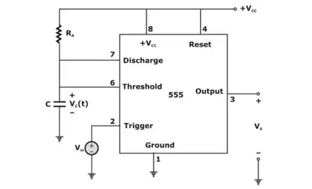 The 555 Circuit connected as Monostable Multivibrator
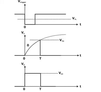 Wave form
The 555 in monostable mode produces a single output pulse of fixed width in response to a negative trigger pulse on the Trigger pin. The external circuit typically comprises one timing resistor R and one timing capacitor C connected between the Discharge pin and ground. The capacitor voltage is monitored by the comparators.

Before a trigger, the Trigger pin is held high (≈ +VCC), the flip-flop is in its quiescent state, the output is low or high depending on convention (see circuit), and Q1 conducts so that the timing capacitor is discharged (VC = 0).

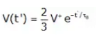
When a negative-going trigger pulse drives the Trigger voltage below VTL = (1/3) VCC, comparator 2 output goes high and sets the flip-flop. The flip-flop output changes state, the discharge transistor Q1 turns off and the timing capacitor begins to charge through R towards VCC.

The capacitor voltage during charging follows the exponential relation
v(t) = VCC (1 - e-t/RC)
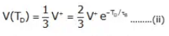
The flip-flop remains in the set state after the trigger finishes (both comparator outputs are then low), so the capacitor keeps charging until its voltage reaches the threshold level VTH = (2/3) VCC. When this happens, comparator 1 forces the flip-flop to reset, the output returns to the quiescent value and Q1 turns on to discharge the capacitor rapidly to near zero volts. The circuit thus returns to the original state, ready for the next trigger.
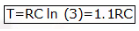
The pulse width T is obtained by solving v(T) = (2/3) VCC using the charging expression. The derivation is shown below.
v(T) = VCC (1 - e-T/RC) = (2/3) VCC
1 - e-T/RC = 2/3
e-T/RC = 1/3
-T/RC = ln(1/3) = -ln 3
T = RC ln 3
The output pulse width therefore depends only on the external time constant RC and is independent of the supply voltage and most internal parameters.
Implementation of Astable Multivibrator using 555 Timer
 Astable Multivibrator 555 Circuit
 Waveform
In astable mode the 555 is configured as a free-running oscillator. The threshold and trigger pins are connected together so the timing capacitor charges and discharges between the two comparator thresholds (1/3 VCC and 2/3 VCC) repeatedly. Two resistors RA and RB and a capacitor C set the timing.
When the capacitor voltage reaches (2/3) VCC, comparator 1 resets the flip-flop, Q1 turns on and the capacitor discharges through RB and Q1 toward ground. When the capacitor voltage falls to (1/3) VCC, comparator 2 sets the flip-flop and Q1 turns off, allowing the capacitor to charge through RA + RB toward VCC. These charge and discharge intervals define the high and low times of the output waveform.

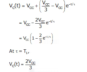
The capacitor charge from (1/3)VCC to (2/3)VCC during the high interval (TC) can be derived as follows.
For charging, the time constant is τC = (RA + RB) C.
The capacitor voltage when charging from an initial value Vi toward VCC is VC(t) = VCC - (VCC - Vi) e-t/τ.
With Vi = (1/3) VCC and VC(TC) = (2/3) VCC we get:
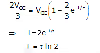
(2/3) VCC = VCC - (2/3) VCC e-TC/τC
(2/3) e-TC/τC = 1/3
e-TC/τC = 1/2
TC = τC ln 2 = (RA + RB) C ln 2
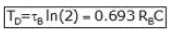
The capacitor discharge from (2/3) VCC to (1/3) VCC during the low interval (TD) follows similarly.
For discharging, the time constant is τD = RB C.
Solving for TD yields:
TD = τD ln 2 = RB C ln 2
The total period and frequency are therefore:
- Total period: T = TC + TD = (RA + 2 RB) C ln 2
- Frequency: f = 1 / T = 1 / [(RA + 2 RB) C ln 2]
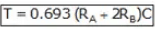

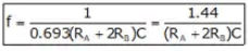
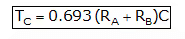
Using ln 2 ≈ 0.693 the commonly used practical forms are:
- TH (high time) = 0.693 (RA + RB) C
- TL (low time) = 0.693 RB C
- T = 0.693 (RA + 2 RB) C
- f = 1 / [0.693 (RA + 2 RB) C]
Duty cycle: Duty cycle is the percentage of the period during which the output is high.
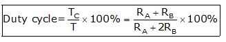
Duty cycle = TH / T = (RA + RB) / (RA + 2 RB) × 100%.
The duty cycle is always greater than 50% for RA > 0. To obtain 50% or less, additional circuits (e.g., a diode across RB or a flip-flop divider) are used.
Active Filters
Active filters are filters that use active components (typically operational amplifiers) along with resistors and capacitors to shape the frequency spectrum of signals. They can provide gain, isolation and improved performance without using inductors.
- An active filter uses amplifying devices such as op-amps, FETs or transistors together with resistors and capacitors.
- A filter is an electronic circuit that modifies the frequency spectrum of an arbitrary signal by selectively passing or attenuating frequency components.
- A filter that produces amplification in its pass band is called an active filter.
- Active filters usually avoid inductors, using resistors and capacitors for frequency selection.
- Active components require biasing (power supplies) and limit the bandwidth of the filter.
- Active filters typically provide higher input impedance and lower output impedance compared with passive designs.
- They are commonly used to suppress unwanted frequency components from information signals and to shape signals for further processing.
Advantages of active filters
- They can provide voltage gain in the pass band.
- They provide isolation between stages due to the buffering action of amplifiers.
- They are easy to cascade because of characteristic impedances of amplifiers.
- They avoid the use of inductors, simplifying design and reducing size and cost for many applications.
Disadvantages of active filters
- Their performance is limited by the amplifier's bandwidth and noise.
- They require external power supplies.
- They dissipate more power and generate heat compared with purely passive networks.
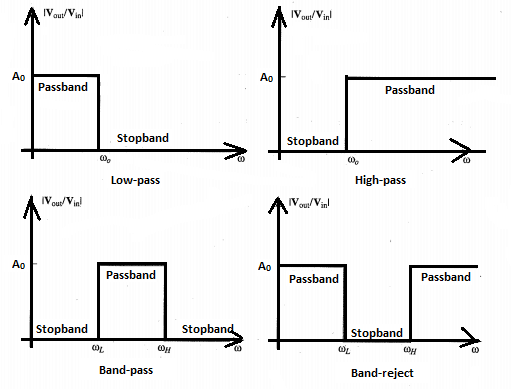
Low Pass Filter (LPF)
- A low-pass filter allows frequencies lower than its cut-off frequency to pass with little attenuation and attenuates higher frequencies.
- It has approximately constant gain from 0 Hz up to the cut-off frequency fH, and at fH the gain falls to 0.707 of the low-frequency gain (-3 dB point).
- Frequencies below fH form the pass band; frequencies above fH form the stop band.
- Common uses include removing high-frequency noise and as anti-aliasing filters before ADCs.
- A single-pole low-pass filter (integrator) is often used to roll off amplifier gain at high frequency to improve stability.
First-order low pass filter circuit:
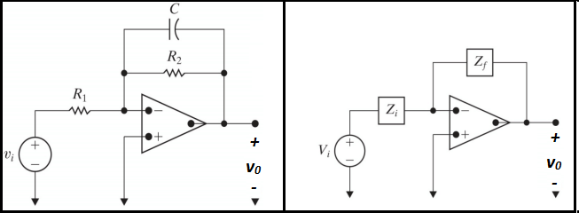
- Transfer function:
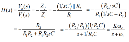
- DC gain: K = R2 / R1
- Cutoff frequency (rad/s): ωc = 1 / (R2 C)
High Pass Filter (HPF)
- A high-pass filter allows frequencies higher than its cut-off frequency to pass and attenuates lower frequencies.
- It is commonly used to remove DC or low-frequency components from signals.
- Single-pole high-pass sections are useful to block DC offsets in amplifiers and single-supply circuitry.
- Filters can be used to separate signals by frequency, passing desired components and attenuating unwanted ones.
First-order high pass filter circuit:
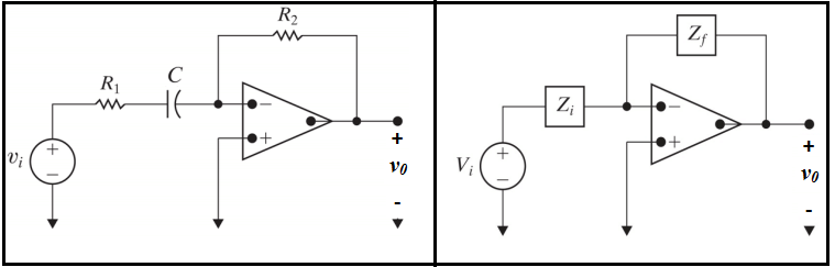
- Transfer function:

- Gain: K = R2 / R1
- Cutoff frequency (rad/s): ωc = 1 / (R1 C)
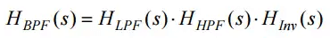
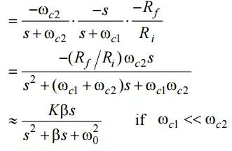
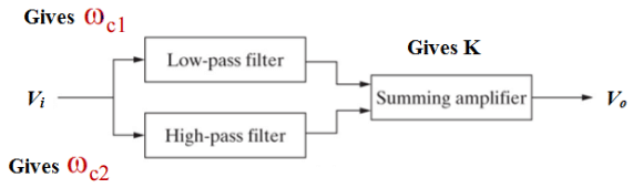
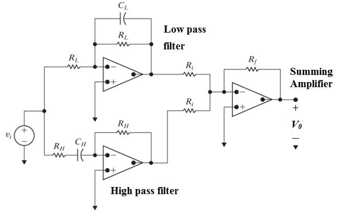
Band Pass Filter (BPF)
- A band-pass filter passes frequencies within a range between a lower cut-off fL and a higher cut-off fH, rejecting frequencies below fL and above fH.
- Cascading a high-pass section with a low-pass section produces a band-pass characteristic.
- The bandwidth of a band-pass filter is BW = fH - fL.
- Simple first-order band-pass filters formed by cascading cannot achieve a very narrow bandwidth; higher-order or resonant designs are used for narrow bands.
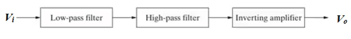
First-order band-pass filter circuit:
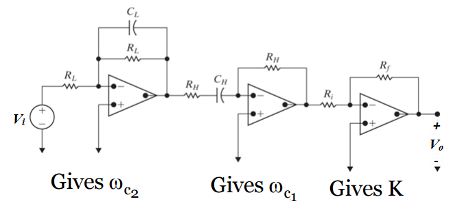
- Transfer function:
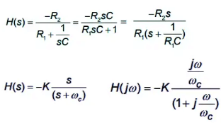
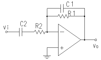
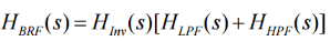
Band Reject Filter (BRF) / Notch Filter
- A band-reject (notch) filter attenuates frequencies within a band between fL and fH while passing frequencies below fL and above fH.
- It is the complement of the band-pass filter and is useful for removing a narrow undesired frequency (for example, mains hum at 50/60 Hz).
First-order band-stop filter circuit:
- Transfer function:
Passive Filters
- A passive filter is constructed solely from passive components: resistors, capacitors and inductors.
Difference between Active and Passive Filters
- Passive filters consist only of passive components and do not provide power gain; active filters include active components and can provide voltage or power gain.
- Active filters require external power supplies; passive filters do not.
- Passive filters may use inductors; active filters typically avoid inductors and use op-amps instead.
- Active filters can provide buffering (isolation) between stages and are easier to cascade; passive filters load adjacent stages.
- Active filters are limited by the amplifier bandwidth and noise; passive filters theoretically have no such amplifier limitations but may be impractical at some frequencies due to inductor size and losses.
- Passive filters are generally more stable at high power and can handle larger currents; active filters dissipate additional power due to their active components.
- Passive filters are often simpler and cheaper for very high-frequency applications; active filters are preferred for low and moderate frequencies where gain and precise characteristics are needed.
FAQs on Timers & Filters
| 1. What is a 555 timer circuit? |  |
| 2. How does a 555 timer circuit work? | |
| 3. What are some common applications of a 555 timer circuit? | |
| 4. Can a 555 timer circuit be used as an active filter? | |
| 5. Are there any limitations or drawbacks of using a 555 timer circuit? | |


 | Explore Courses for Electronics and Communication Engineering (ECE) exam |
 | Get EduRev Notes directly in your Google search |